
What you need to know about analog keys and multiplexers
For about twenty-five years, integrated semiconductor analog keys and multiplexers created on their basis are faithfully serving the developers of electronic products. The manufacturing process was improved, the chip design changed - all this allowed to reduce the supply voltage, power consumption, the resistance of the public key, the injected charge, the switching time. What is interesting is the company Maxim in this group of 325 devices.
The architecture of keys and multiplexers has not changed much over many years, but the constant demand for improved performance forces manufacturers to develop more and more devices to meet the demands of developers. For a long time, MOS (metal-oxide-semiconductor) transistors were used as analog keys. Possessing low resistance in the conducting state and extremely high resistance in the cutoff state, with small leak points and small capacitance, they were almost ideal analog voltage-controlled keys. The need to switch signals equal or close in magnitude to the supply voltage made it necessary to solve this problem by using switches on complementary MOSFETs (CMOS). Known circuitry 4066 is a classical analog circuit for signals in the range from ground to positive supply voltage (Maxim manufactures this microchip called MAX4066). It is controlled by a unipolar signal from logic chips. A single p-channel or p-channel FET operating in the enrichment mode can serve as an analog key, but its resistance in the open state will depend significantly on the value of the switched signal.
The connection of the n-channel and p-channel MOSFETs in parallel sharply reduces this dependence. Only one condition is necessary - switching on and switching off these transistors should be carried out simultaneously. Long-term improvements in the analog key based on CMOS transistors have lowered the switching voltage threshold to 2.5-5.0 V. The addition of a level converter has allowed obtaining gate control signals of complementary MOSFETs from input signals of a logic level. At the same time, the analog key can now switch the analog signal by ± 15 V. The scheme of the modern key is shown in Fig. 1.
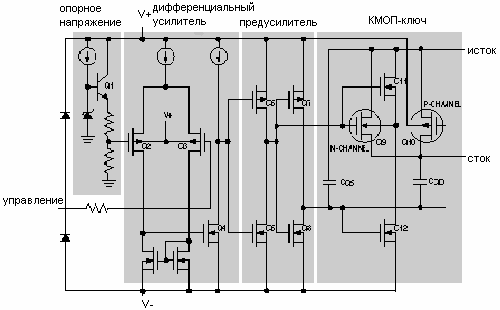
Fig. 1. Diagram of a modern CMOS key
The control signal has a TTL logic level. In this case, the CMOS switch on transistors Q9 and Q10 can transmit analog signals with a level of ± U pit . The transistors Q11 and Q12 shown in the diagram improve the operation of the key, reducing leakage of the key and decreasing the modulation of the resistance of the open channel. These two transistors should never be turned on at the same time. Otherwise, the negative power bus will be connected to the load and the on / off time will increase. The safety mode of operation of transistors Q11 and Q12 should be provided constructively. Fairly good parameters for the value of the public key resistance, for leakage currents and dynamic distortions of transmission of a large signal at a frequency of up to 500 KHz are implemented in MAX3XX keys. The simplest way to improve the above parameters is to connect the parallel to the keys on the chip. So MAX351, having 4 keys, with parallel connection has typical resistance in the open state of 5.5 Ohm and maximum - 11.25 Ohm. In this case, the maximum change in the key resistance from the change in the value of the switched signal does not exceed ΔR open ≤ 1,25 Ohm.
The current of the switched signal flows through the open transistors of the switch. From power sources, there is practically no current flowing into the key. But to displace the levels and to control the key, the current is needed.
The increase in current occurs at a voltage of about 0.8 V and 2.4 V, which is due to the transition of transistors from the open state to the closed state (and vice versa) and their transition to this time into a linear regime. If the logical and analog voltage of the power supplies are equal, then the currents flow through the microcircuit at the leakage current level of less than 1 μA. For normal operation of a switch with different voltages (for example, +5 V and ± 15 V), it is necessary to place shunt capacitors of 10 μF in parallel with 100 nF to each source terminal.
The dynamic errors of the keys are determined by the fact that the control signal passes through several stages and each has a delay. This is especially important in multi-channel multiplexers, for example, 8 in 1. It is not possible to implement the channel on, unless the previous one is turned off. That's why, in the MAX338 chip, a guaranteed delay time for switching is structurally introduced - at least 10 nsec. When the key is turned on and off, the control signal through the capacitance of the transistors of the pre-cascades injects some charge into the conductive channel of the key. This leads to an error in the transmission of the signal through the key. The size of the injected charge is the smaller, the smaller the resistance of the open channel. For the same reasons, the rise and fall time of the logical input signal for most key MAXIM circuits should not exceed 20 nsec.
Knowing the fineness of key construction, their strengths and weaknesses, one can find the widest application of semiconductor keys and multiplexers in radio electronic equipment. They can operate with radio frequencies up to 1 MHz and higher. Most analog keys allocate little power dissipation and require a simple logical interface. The operation of the keys depends on the signal current in the switching element and, in order to reduce transmission losses, is usually limited to milliamperes.
To reduce crosstalk at frequencies of the order of 10 MHz and higher, you can use keys (standard MAX312, MAX383, video T-keys MA4545) connected in T-mode (Figure 2). One or two switches are connected to ground with low resistance (typical -40 Ohm) and an excellent decoupling factor (-80 dB per 10 MHz). However, it must be remembered that with increasing the operating frequency of the signal, crosstalk and isolation become unsatisfactory.
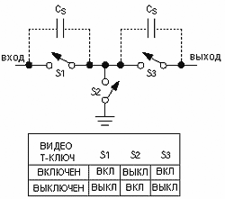
Fig. 2. T-shaped circuit for turning on the key for a 10 MHz signal
A simple oscillator circuit for 2 frequencies stabilized by quartz resonators is obtained by using a chip with four keys (MAX 383) with a supply of ± 8 V or, with MAX 411, ± 18 V.
Very useful may be integrated circuits of keys and multiplexers with automatic setting of gain, frequency, phase or voltage. For example, if you apply a signal to the non-inverting input of an operational amplifier and output a series resistive matrix, then using a 16-channel MAX 306 multiplexer, you can select one of 16 gain levels. In this case, each key on one side is connected to its "own" resistor, and the second side of all keys is combined and connected to the inverting input of the operational amplifier.
A wide use was found for analog keys in sound systems. When passing a signal through the key, there should be no deterioration of the signal, the introduction into it of any new information, distortion of the shape and phase of the waves. Completely avoid this can not. Obviously, all distortions must be minimized. The total value of the coefficient of nonlinear distortion (THD) is defined as the ratio of the square root of the sum of the squares of the second, third and higher harmonics to the value of the fundamental (first) harmonic. The choice of an analog key with a minimum of THD requires one - a low resistance in the open state (R on ) and, consequently, a slight unevenness of the resistance R on or flatness.
The flatness is defined as the difference between the maximum and minimum values of the resistance in the open state measured in the specified range of the analog signal. Often, (unless otherwise specified in the documentation), flatness is assumed to be 10% of the resistance of the open channel. Distortions are the result of parallel connection of the p and n-channel transistors, which have non-linear resistance characteristics in the open state.
In practice, the maximum of nonlinear distortions is determined by the following relation:

Where R is the load. - the load included in series with the key.
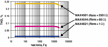
Fig. 3. Dependence of the total coefficient of nonlinear distortion (THD) for the frequency
In Fig. 3 shows the frequency dependence of THD for three MAX 4501, MAX4544, and MAX4621 with the test load R of the load. = 10 kOhm.
These graphs show that in sound systems, to minimize the total nonlinear distortion, it is necessary to select keys with very low resistance in the open state.
CMOS analog keys have undoubtedly many useful qualities, so most developers consider them to be the norm and use them in a wide variety of applications.
Let's pay attention to some technical parameters of the keys. Today, there are many analog keys that work with one low-voltage power source. Low-voltage switches with unipolar power supply and logic signals according to CMOS standards and TTL levels are also used. But there are also keys that operate on ± 15 V or ± 12 V power. To control them, another power supply is required, labeled V L , which is usually 5 V or 3.3 V.
If the logic signal is at the level of V + (or V L , if present), then the current from the power supply is not substantially flowing through the analog keys. Applying TTL levels at a five-volt voltage V L , it is possible to increase the current from the power supply by more than 1000 times. To avoid unnecessary current consumption from the power source, you should avoid using TTL levels - inheritance of the 1980s.
Switching times (t-on and t-off) for most analog keys are in the range of 60 nsec. Up to 1 msec.
For MAXIM "bezchelchechkovyh" sound switches, switching time is increased to a millisecond range, which will eliminate audible sound clicks.
So, we see that to transmit a signal with minimal distortion, you need either a minimum key resistance in the open state, or the maximum possible load at the key output. Let's consider one more aspect when switching - the effect of charge injection. To obtain a low value of R ON, an extension of the channel region is required. The result is a large input capacitance and a corresponding board: an increase in dissipated power from the charge-discharge current in each switching cycle. The constant charge time t = R × C depends on the resistance (R ON ) and the capacity (C) of the load. This usually lasts a few dozen nanoseconds, but low-resistance keys have a longer duration of on and off times. Keys with high R ON are faster. MAXIM offers both types of keys - with the same pinout and in the same SOT-23 package. The MAX4501 and MAX4502 have a higher resistance R ON , but the short on / off time of the MAX4514 has a lower resistance R ON , but a longer switching time.
Another negative consequence of low-ohmic keys is a higher level of charge injection, caused by an increased current level through the gate capacitance. This is especially important when using keys in sampling / storage devices for accurate conversion to an ADC.
The protection of electrostatic charge keys (ESD) is based on the achievements of MAXIM in this field. They allowed to increase the protection of new analog keys to ± 15 kW according to the recommendations of IEC 1000-4-2 level 4 (the highest level). All analog inputs for ESD tests use the human body model, as well as contact and discharge through the air gap specified in the IEC 1000-4-2 methodology.
Thus, the produced MAX4551-MAX4553 keys are pin-compatible with most standard four key chips such as the DS201 / 211, MAX391, etc. Now it is not necessary to protect the analog inputs with expensive limiting diodes, as protection against electrostatic discharges (up to 15 KV) is embedded in the scheme of keys and multiplexers.
The next important characteristic should be noted in modern keys. Typically, the allowable range of the input signal voltage is limited by the voltage on the power supply rails. If the analog signal exceeds the voltage of the power supply, then current flows through the back-biased parasitic diodes. In the case where this current is not limited, the chip is out of order due to overheating. Therefore, most old keys and multiplexers could work with currents not exceeding 10-20 mA.
New keys MAXIM'a have built-in protection against breakdown, when they remain operative up to ± 25 V (some up to 36 V) of the input signal with a power supply of 15 V and ± 40 V with power off. In this case (at overvoltage) on the analog signal input, the key takes a high impedance regardless of the key state or the load resistance. Only the leakage current constituting the nanoamperes can flow from the signal source. Here one thing is very important: these keys do not require a specific order of supply voltage and analog signal voltage. Even with the power removed, there is no breakdown of the key from the analog signal. The break-proof keys MAX4511 ÷ MAX4513 on the pins are compatible with the DS411 ÷ DS413.
In a brief journal article it is impossible to make a detailed description of all the properties of keys and multiplexers. To all who are interested in such information, I propose to visit the site www.maxim-ic.cоm or the site of the official distributor of MAXIM - the company Rainbow Technologies. At these addresses you will find a lot of useful for the correct choice and use of this type of instrument.

Comments
When commenting on, remember that the content and tone of your message can hurt the feelings of real people, show respect and tolerance to your interlocutors even if you do not share their opinion, your behavior in the conditions of freedom of expression and anonymity provided by the Internet, changes Not only virtual, but also the real world. All comments are hidden from the index, spam is controlled.