
Optocouplers and their application
Introduction
History
The idea of creating and using optocouplers dates back to 1955, when Loebner EE "Optoelectronic devices network" offered a whole series of devices with optical and electrical connections between the elements, which allowed amplification and spectral conversion of light signals, creating devices with two stable states - bistable optocouplers, optoelectronic devices for accumulation and storage of information, logic circuits, shift registers. The term "optocoupler" was also proposed there, formed as an abbreviation for the English "optical-electronic device".
The optocouplers described in this work, perfectly illustrating the principles, proved to be unsuitable for industrial implementation, since they were based on an imperfect elementary base-inefficient and inertial powder electroluminescent capacitors (emitter) and photoresistors (receiver). The most important performance characteristics of the instruments were also incomplete: low-temperature and temporary stability of parameters, insufficient resistance to mechanical influences. Therefore. At first the optocoupler remained only an interesting scientific achievement not finding use in engineering.
Only in the mid-1960s the development of semiconductor light-emitting diodes and technologically advanced high-efficiency fast-acting silicon photodetectors with pn-junctions (photodiodes and phototransistors) began to create an elementary base of modern optronic technology. By the early 1970s, the production of optocouplers in the leading countries of the world had become an important and rapidly developing branch of electronic technology, successfully complementing traditional microelectronics.
Basic Definitions
Optocouplers are optoelectronic devices with a source and a radiation receiver (light emitter and photodetector) with some kind of optical and electrical connection between them, structurally related to each other.
The principle of operation of optocouplers of any kind is based on the following. In the radiator, the energy of the electrical signal is converted to light, in the photodetector, on the contrary, the light signal causes an electrical response.
In practice only optocouplers have received propagation, which have a direct optical connection from the radiator to the photodetector and, as a rule, all kinds of electrical connection between these elements are excluded.
According to the degree of complexity of the structural diagram, two groups of devices are distinguished from the products of optocouplers. The optocoupler (also referred to as the "elementary optocoupler") is an optoelectronic semiconductor device consisting of a radiating and photodetective elements, between which there is an optical connection that provides electrical isolation between the input and the output. The optoelectronic integrated microcircuit is a microchip consisting of one or more optocouplers and one or more matching or amplifying devices electrically connected to them.
Thus, in an electronic circuit such a device performs the function of a communication element, in which, at the same time, an electrical (galvanic) isolation of the input and output is performed.
Distinctive features of optocouplers
The advantages of these devices are based on the general optoelectronic principle of using electrically neutral photons for information transfer. The main ones are:
- The possibility of providing an ideal electrical (galvanic) decoupling between the input and output; For optocouplers, there are no fundamental physical or constructive limitations to achieve arbitrarily high voltages and resistance to decoupling and arbitrarily small throughput;
- The possibility of implementing contactless optical control of electronic objects and the resulting diversity and flexibility of design solutions for control circuits;
- Unidirectionality of information spreading through the optical channel, absence of a reciprocal response of the receiver to the radiator;
- Wide frequency bandwidth of the optocoupler, no restriction on the low frequency side (which is characteristic of pulse transformers); The possibility of transmission along the optocoupler circuit, both a pulse signal and a constant component;
- The possibility to control the output signal of the optocoupler by acting (including non-electric) on the material of the optical channel and the consequent possibility of creating a variety of sensors, as well as various devices for transmitting information;
- The possibility of creating functional microelectronic devices with photodetectors whose characteristics under illumination vary according to a complex predetermined law;
- The immunity of optical communication channels to the effect of electromagnetic fields, which in the case of "long" optocouplers (with an extended optical fiber light guide between the radiator and the receiver) makes them immune from interference and information leakage, and also excludes mutual pick-ups;
- Physical and structural-technological compatibility with other semiconductor and microelectronic devices.
Optocouplers also have certain drawbacks:
- Significant power consumption due to the need for double conversion of energy (electricity - light - electricity) and low efficiency of these transitions;
- Increased sensitivity of parameters and characteristics to the effects of high temperature and penetrating nuclear radiation;
- More or less noticeable temporary degradation (deterioration) of parameters;
- A relatively high level of intrinsic noise, due, as with the previous two drawbacks, to the peculiarities of the physics of light-emitting diodes;
- The complexity of feedback realization caused by the electrical disconnection of the input and output circuits;
- Structural and technological imperfection associated with the use of hybrid non-planar technology, (with the need to combine several - separate crystals from various semiconductors, located in different planes).
The listed shortcomings of optocouplers with the improvement of materials, technology, circuitry are partially eliminated, but, nevertheless, for a long time will be quite fundamental in nature. However, their merits are so high that they ensure a confident non-competitiveness of optocouplers among other devices of microelectronics.
Generalized structural scheme
As an element of communication, the optocoupler is characterized by the transmission coefficient K i , determined by the ratio of the output and input signals, and the maximum information transfer rate F. Practically, instead of F, the rise and fall times of the transmitted pulses tpp (cn) or the cut-off frequency are measured. The capabilities of the optocoupler as an element of galvanic isolation are characterized by maximum voltage and resistance of decoupling U razv and R razv and throughput capacitance C razv.
In the structural diagram in Fig. 1 input device serves to optimize the operating mode of the emitter (for example, the shift of the LED to the linear portion of the watt-ampere characteristic) and the conversion (amplification) of the external signal. The input unit must have a high conversion efficiency, high speed, a wide dynamic range of admissible input currents (for linear systems), a small value of the "threshold" input current, at which reliable information transmission through the circuit is ensured.
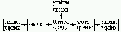
Figure 1. Generalized structure of the optocoupler
The purpose of the optical medium is to transfer the energy of the optical signal from the emitter to the photodetector, and in many cases to ensure the mechanical integrity of the structure.
The principal possibility of controlling the optical properties of a medium, for example, by using electro-optical or magneto-optical effects, is reflected by the introduction of a control device into the circuit. In this case we obtain an optocoupler with a controlled optical channel, functionally different from the "ordinary" optocoupler: the output signal can be varied both in Input, and control circuit.
In the photoreceiver, the information signal is "recovered" from the optical signal to the electric signal; While striving to have high sensitivity and high speed.
Finally, the output device is designed to convert the signal of the photodetector to a standard shape, convenient for influencing the subsequent cascades of the optocoupler. A practically mandatory function of the output device is signal amplification, since the losses after double conversion are very significant. Often, the photoreceiver performs the amplification function (for example, a phototransistor).
The general block diagram of Fig. 1 is realized in each specific device only by a part of the blocks. In accordance with this, three main groups of optronic devices are distinguished; Previously named opto-couplers (elementary optocouplers), using light-emitting unit - optical medium - photodetector; Optoelectronic (optron) microcircuits (optocouplers with the addition of an output, and sometimes an input device); Special types of optocouplers - devices that functionally and structurally differ substantially from elementary optocouplers and optoelectronic ICs.
A real optocoupler can be arranged and more complicated than the circuit in Fig. 1; Each of said blocks may include not one but several identical or similar elements connected electrically and optically, however this does not substantially change the fundamentals of the optronics electronics and electronics.
Application
As optoelectronic isolation elements, optocouplers are used: for communication between equipment units, between which there is a significant difference in potentials; To protect input circuits of measuring devices from interference and interference, etc.
Another important field of application of optocouplers is optical, noncontact control of high-current and high-voltage circuits. The launch of powerful thyristors, triacs, triacs, control of electromechanical relay devices.
A specific group of control optocouplers are resistor optocouplers, designed for low-current switching circuits in complex devices for visual display of information performed on electroluminescent (powder) indicators, mimic diagrams, screens.
The creation of "long" optocouplers (devices with an extended flexible fiber-optic lightguide) has opened up a completely new direction of application of products of optronic technology - communication at short distances.
Various optocouplers (diode, resistor, transistor) are used in purely radio engineering schemes of modulation, automatic gain control, etc. The effect on the optical channel is used here to output the circuit to the optimum operating mode, for contactless tuning of the regime, etc.
The possibility of changing the properties of the optical channel under various external influences on it allows the creation of a whole series of optocouplers: such as moisture and gas sensors, a sensor for the presence of a liquid in the volume, sensors for the purity of surface treatment of an object, the speed of its movement,
The use of optocouplers for energy purposes, ie, the operation of a diode optocoupler in the photovoltaic regime, is quite specific. In this mode, the photodiode generates electrical power in the load and the optocoupler is to a certain extent similar to a low-power secondary power source completely decoupled from the primary circuit.
The creation of optocouplers with photoresistors, whose properties under illumination vary according to a given complex law, allows modeling mathematical functions, is a step towards the creation of functional optoelectronics.
The universality of optocouplers as elements of galvanic isolation and contactless control, the diversity and uniqueness of many other functions are the reason that the spheres of application of these devices are computer technology, automation, communication and radio equipment, automated control systems, measuring equipment, control and regulation systems, medical electronics , Devices for visual display of information.
Physical basis of optocouplers
Element base and device of optocouplers
The elemental basis of optocouplers consists of photodetectors and radiators, as well as the optical medium between them. All these elements are subject to such general requirements as small size and weight, high durability and reliability, resistance to mechanical and climatic influences, manufacturability, low cost. It is also desirable that the elements are sufficiently broad and long-term industrial approbation.
Functionally (as an element of the circuit), the optocoupler is characterized primarily by what type of photodetector it is used in.
The successful use of a photodetector in an optocoupler is determined by the fulfillment of the following basic requirements: the efficiency of converting the energy of radiation quanta to mobile electric energy; The presence and effectiveness of internal built-in amplification; High speed; Breadth of functionality.
In optocouplers, photodetectors of various structures sensitive in the visible and near infrared regions are used, since it is in this spectral range that there are intense radiation sources and photodetectors can be operated without cooling.
The most universal are photodetectors with pn junctions (diodes, transistors, etc.), in the overwhelming majority of cases they are made on the basis of silicon and the region of their maximum spectral sensitivity is close to l = 0.7 ... 0.9 μm .
Numerous requirements are also imposed on the radiators of optocouplers. The main ones are: spectral matching with the selected photodetector; High efficiency of converting the energy of electric current into energy of radiation; Preferential radiation direction; High speed; Simplicity and convenience of excitation and modulation of radiation.
For use in optocouplers, several types of radiators are suitable and available:
- Miniature incandescent light bulbs .
- Neon light bulbs , which use the glow of an electric discharge of a neon-argon gas mixture.
These types of radiators are characterized by low light output, low resistance to mechanical influences, limited durability, large dimensions, complete incompatibility with integrated technology. Nevertheless, in some types of optocouplers they can be used. - The powder electroluminescent cell uses as a luminous body fine crystalline grains of zinc sulphide (activated by copper, manganese or other additives) suspended in a polymerizable dielectric. When sufficiently high AC voltages are applied, the pre-breakdown luminescence process proceeds.
- Thin film electroluminescent cells . The glow is associated with the excitation of manganese atoms by "hot" electrons.
Both powder and film electroluminescent cells have a low efficiency of converting electrical energy into light, low durability (especially thin films), are difficult to control (for example, the optimal regime for powdery phosphors is ~ 220 V at f = 400 ... 800Hz). The main advantage of these radiators is the constructive technological compatibility with photoresistors, the possibility of creating on this basis multifunctional, multi-element optronic structures.
The main most universal type of radiator used in optocouplers is a semiconductor injection light-emitting diode (LED). This is due to its following advantages: high efficiency of conversion of electrical energy into optical energy; Narrow emission spectrum (quasi-monochromaticity); The latitude of the spectral range overlapped by different LEDs; Radiation direction; High speed; Low values of supply voltages and currents; Compatibility with transistors and integrated circuits; Simplicity of modulating the radiation power by changing the forward current; The ability to work both in pulsed and continuous mode; Linearity of the watt-ampere characteristic in a more or less wide range of input currents; High reliability and durability; Small size; Technological compatibility with microelectronics products.
The general requirements for the optical immersion medium of an optocoupler are as follows: high refractive index n; High value of resistivity r im ; High critical field strength E im kp , sufficient heat resistance Dq im slave ; Good adhesion with crystals of silicon and gallium arsenide; Elasticity (this is necessary, since it is not possible to align the elements of the optocoupler with the coefficients of thermal expansion); Mechanical strength, since the immersion medium in the optocouple performs not only light-transmitting, but also structural functions; Manufacturability (ease of use, reproducibility of properties, cheapness, etc.).
The main type of immersion medium used in optocouplers is polymer optical adhesives. For them it is typical n im = 1,4 ... 1,6, r im > 10 12 ... 10 14 Ohm cm, E im kp = 80 kV / mm, Dq im slave = -60 ... 120 C. Adhesives have good adhesion to silicon and gallium arsenide, combine high mechanical strength and resistance to thermal cycling. Non-hardening vaseline-like and rubber-like optical media are also used.
Physics of energy conversion in a diode optocoupler
Consideration of the processes of energy conversion in an optocoupler requires taking into account the quantum nature of light. It is known that electromagnetic radiation can be represented as a stream of particles - quanta (photons), energy. Each of which is defined by the relation:
E φ = hn = hc / n l (2.1)
Where h is the Planck constant;
C is the speed of light in a vacuum;
N is the refractive index of the semiconductor;
N, l - frequency of oscillations and wavelength of optical radiation.
If the flux density of quanta (that is, the number of quanta passing through unit of area per unit time) is Np, then the total specific radiation power is:
P Φ = N Φ * E Φ (2.2)
And, as is clear from (2.1), for a given N , it is the larger, the shorter the wavelength of the radiation. Since in practice P Φ (the energy irradiance of the photodetector) is given, the following relation
N φ = P ф / Е ф = 5 * 10 15l P ф (2.3)
Where N φ , cm -2 s -1 ; L , μm; P f , mW / cm.
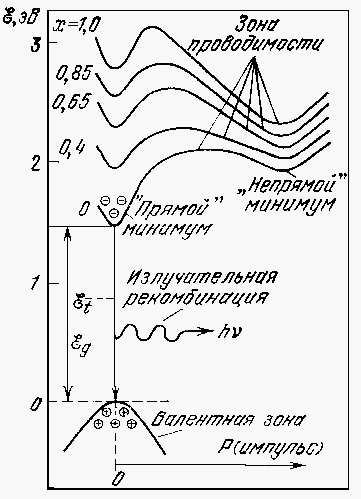
Fig. 2. Energy diagram of a direct-gap semiconductor (based on the example of a ternary GaAsP compound)
The mechanism of injection luminescence in an LED consists of three main processes: radiative (and nonradiative) recombination in semiconductors, injection of excess minority carriers into the LED base, and emission of radiation from the generation region.
Recombination of charge carriers in a semiconductor is determined, first of all, by its zone diagram, by the presence and nature of impurities and defects, by the degree of disturbance of the equilibrium state. The main materials of optocouplers (GaAs and ternary compounds based on it GaA1As and GaAsP) belong to direct-gap semiconductors, i.e. To those in which direct optical band-to-band transitions are allowed (Fig. 2). Each act of recombination of the charge carrier according to this scheme is accompanied by the emission of a quantum whose wavelength, in accordance with the law of conservation of energy, is determined by the relation:
L ile [μm] = 1.23 / E φ [eB] (2.4)
It should be noted that there are also competing nonradiative - recombination mechanisms. Among the most important of them are:
- Recombination at deep centers. The electron can pass into the valence band not directly, but through certain recombination centers, which form the allowed energy levels in the band gap (level E t in Fig. 2).
- Auger recombination (or shock). At very high concentrations of free charge carriers, the probability of a collision of three bodies increases in the semiconductor, the energy of the recombining electron-hole pair is then given to the third free carrier in the form of kinetic energy, which it gradually dissipates in collisions with the lattice.
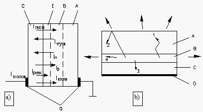
Fig. 3. Electrical (a) and optical (b) LED model. A is the optically "transparent" part of the crystal; B - the active part of the crystal; C is the "opaque" part of the crystal; D - ohmic contacts; E - space charge region
The relative role of various recombination mechanisms is described by introducing the concept of the internal quantum yield of the radiation h int , determined by the ratio of the probability of radiative recombination to the total (radiative and nonradiative) recombination probability (or, otherwise, the ratio of the number of generated quanta to the number of minority carriers injected at the same time). The value of h int is the most important characteristic of the material used in the LED; It is obvious that 0 ![]() H int
H int ![]() 100%.
100%.
The creation of an excess concentration of free carriers in the active (radiating) region of the LED crystal is carried out by injecting them with a pn junction biased in the forward direction.
A "useful" component current that supports radiative recombination in the active region of the diode is the electron current I n (Fig. 3a) injected by the pn junction. The "useless" components of the forward current are:
- The hole component I p , due to the injection of holes into the n-region and reflecting the fact that there are no p-n junctions with one-sided injection, the fraction of this current is the less the n-region is more doped than the p-region.
- The recombination current (nonradiative) in the space charge region of the p - n junction of the I rivers . In semiconductors with a large band gap at small direct displacements, the fraction of this current can be appreciable.
- Tunnel current I tun due to "leakage" of charge carriers through a potential barrier. The current is carried by the main carriers and does not contribute to the radiative recombination. The tunnel current is greater than the pn junction, it is noticeable for a strong degree of doping of the base region and for large direct displacements.
- The current of surface leakage I n due to the difference in the properties of the surface of the semiconductor from the properties of the volume and the presence of certain short-circuiting inclusions.
The efficiency of the pn junction is characterized by the injection coefficient:
(2.5) |
Obviously, the limits of a possible change of g are the same as for h int , that is, 0 ![]() G
G
![]() 100%.
100%.
In the emission of radiation from the generation region, the following types of energy losses occur (Fig. 3b):
- Losses on self-absorption (rays 1). If the wavelength of the generated quanta exactly corresponds to formula (2.4), then it coincides with the "red absorption boundary" (see below), and such radiation is rapidly absorbed in the semiconductor thickness (self-absorption). In reality, radiation in direct-band semiconductors does not follow the ideal scheme given above. Therefore, the wavelength of the generated quanta is somewhat larger than in accordance with (2.4):
- Loss of total internal reflection (rays 2). It is known that when rays of light fall on the interface between an optically dense medium (semiconductor) and the optically less dense (air) for a part of these rays, the condition of total internal reflection is satisfied, such rays reflected inside the crystal are ultimately lost due to self-absorption.
- Losses on the reverse and face radiation (beam 3 and 4).
Quantitatively, the efficiency of the output of optical energy from the crystal is characterized by the output factor K determined by the ratio of the radiation power output in the desired direction to the radiation power generated inside the crystal. Just as for the coefficients h int and g , the condition 0 ![]() To wholesale
To wholesale ![]() 100%.
100%.
G.
The integral indicator of the emissivity of the LED is the magnitude of the external quantum output h ext . It is clear from the above that h ext = h intg K opt .
Let's go to the receiving block. The principle of operation of photodetectors used in optocouplers is based on the internal photoelectric effect, which consists in the separation of electrons from atoms inside the body under the action of electromagnetic (optical) radiation.
Quanta of light, being absorbed in a crystal, can cause the electrons to separate from atoms, both the semiconductor itself and the impurity. In accordance with this, one speaks of one's own (unmixed) and impurity absorption (photoelectric effect). Since the concentration of impurity atoms is small, photoelectric effects based on intrinsic absorption are always more important than those based on the impurity one. All photodetectors used in optocouplers "work" on a pure photoelectric effect. In order for the quantum of light to cause the electron to detach from the atom, it is necessary to fulfill the obvious energy relations:
E ф1 = hn 1  E c - E v (2.6)
E ф2 = hn 2 E c - E t (2.7)
Thus, an intrinsic photoeffect can only take place when a radiation with a wavelength less than a certain value of lp is applied to the semiconductor:
Lgr = hc / (E c - E v )  1.23 / E g (2.8)
The second equality in (2.8) is valid if l gr is expressed in micrometers, and the width of the forbidden band of the semiconductor is E g in electronovolts. The quantity lp is called the long-wave or "red" boundary of the spectral sensitivity of the material.
The intensity of the photoelectric effect (in that spectral region where it can exist) depends on the quantum yield, determined by the ratio of the number of electron-hole pairs generated to the number of absorbed photons. Analysis of the experimental dependences on shows that in the spectral region interesting for optocouplers, b = 1.
The formation of free charge carriers under the influence of irradiation is manifested in the semiconductor in the form of two photoelectric effects: photoconductivity (an increase in the conductivity of the sample under illumination) and photovoltaic (the appearance of a photo-emf in a pn junction or other form of a potential barrier in a semiconductor under illumination). Both effects are used in the practice of designing photodetectors; For optocouplers, the use of the photo-emf effect is preferable and dominant.
The main parameters and characteristics of photodetectors (irrespective of the physical nature and design of these devices) can be divided into several groups. Optical characteristics include the area of the photosensitive surface, the material, the size and configuration of the optical window; Maximum and minimum radiation power levels. To electro-optical - photosensitivity, the degree of homogeneity of the distribution of sensitivity on the photodetector pad; The spectral density of sensitivity (the dependence of the parameter characterizing the sensitivity on the wavelength); Own noise of the photodetector and their dependence on the level of illumination and the range of operating frequencies; Resolving time (speed); Quality factor (combined indicator, allowing to compare different photodetectors with each other); Linearity index; Dynamic range. As an element of the electrical circuit, the photodetector is characterized primarily by the parameters of its equivalent circuit, the requirements for operating modes, the presence (or absence) of the built-in amplification mechanism, the type and shape of the output signal. Other characteristics: operational, reliability, dimensional, technological - nothing specific "photoreceiver" does not contain.
Depending on the nature of the output signal (voltage, current), one speaks of the volt or current sensitivity of the receiver S, measured respectively in V / W or A / W. The linearity (or nonlinearity) of the photodetector is determined by the value of the exponent n in the equation connecting the output signal to the input signal: Uout (or Iout) ~ P f . For n ![]() 1 photodetector is linear; The range of Pf (from Pfmax to Pfmin) in which this is done determines the dynamic range of the linearity of the photodetector D , usually expressed in decibels: D = 10 lg (Pf max / Pf min ).
1 photodetector is linear; The range of Pf (from Pfmax to Pfmin) in which this is done determines the dynamic range of the linearity of the photodetector D , usually expressed in decibels: D = 10 lg (Pf max / Pf min ).
The most important parameter of the photodetector, which determines the threshold of its sensitivity, is the specific detecting power D, measured in W -1 m Hz 1/2 . At a known value of D, the sensitivity threshold (the minimum fixed radiation power) is defined as
P f min =  / D (2.9)
Where A is the area of the photosensitive site; D f - the range of operating frequencies of the photo signal amplifier. In other words, the parameter D plays the role of the photodetector quality factor.
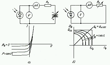
Fig. 4. Measurement schemes and families of volt-ampere characteristics in photodiode (a) and photoentile (b) modes of operation of a diode
As applied to optocouplers, not all of the listed characteristics are equally important. As a rule, photodetectors in optocouplers operate under irradiations very far from the threshold, so the use of the parameters P f min and D is practically useless. Structurally, the photodetector in the optocoupler is usually "drowned" in immersion. The environment connecting it with the radiator, therefore the knowledge of the optical characteristics of the input window loses its meaning (as a rule, there is no such window specially). It is not very important to know the sensitivity distribution on the photosensitive pad, since the integral effects are of interest.
The mechanism of operation of photodetectors based on the photovoltaic effect is considered using the example of planar-epitaxial photodiodes with a pn junction and with a p-in structure, in which an n + substrate, an n- or i-type base (weak conductivity n Type) and a thin p + layer. When operating in the photodiode regime (Fig. 4a), the exerted voltage causes the mobile holes and electrons to escape from the pn (p - i) junction; The picture of the field distribution in the crystal turns out to be sharply different for the two structures under consideration.
The light radiation, being absorbed in the base region of the diode, generates electron-hole pairs that diffuse to the pn junction, are separated by it and cause the appearance of an additional current in the external circuit. In p-i-n-diodes, this separation takes place in the field of i-field, and instead of the diffusion process, charge carriers drift under the influence of the electric field. Each generated electron-hole pair that has passed through the pn junction causes a charge in the external circuit to be equal to the charge of the electron. The more irradiation of the diode, the more photocurrent. The photocurrent flows also when the diode is displaced in the forward direction (Fig. 4, a), but even at low voltages it is much less than the forward current, so its isolation is difficult.
The working region of the current-voltage characteristics of a photodiode is the third quadrant in Fig. 4, a; Accordingly, as the most important parameter, the current sensitivity
 |
(2.10) |
The second equality in (2.10) was obtained under the assumption of the linear dependence I ф = f (P ф ), and the third under the condition of ignoring the dark current (I T << I Ф ), which is usually satisfied for silicon photodiodes.
If we illuminate the photodiode without applying an external displacement to it, then the process of separation of the generated electrons and holes will proceed due to the action of the intrinsic built-in field of the pn junction. In this case, the holes will flow into the p-region and partially compensate for the built-in field of the pn junction. A new equilibrium state (for a given value: P ф ) is created in which a photo-emf appears on the external terminals of the diode. If you close the illuminated photodiode for some load, it will give it a useful electrical power Р э .
Characteristic points of the current-voltage characteristics of a diode operating in such a photovoltaic mode are the EMF of idling Uxx and the short-circuit current Ic (Figure 4, b).
Schematically, the photodiode in the gate mode works as a kind of secondary power source, so its determining parameter is the efficiency of conversion of light energy into electrical:
Efficiency = P e / AP ф = aU xx I кз / A pф (2.11)
In the photovoltaic regime, an important class of photovoltaic devices-solar cells-operates.
Parameters and characteristics of optocouplers and optoelectronic integrated circuits
Classification of parameters of optronic devices
When classifying the products of optocouplers, two things are taken into account: the type of photodetector device and the design features of the device as a whole.
The choice of the first classification feature is due to the fact that almost all optocouplers have an LED at the input, and the functionality of the device is determined by the output characteristics of the photodetector device.
As a second feature, a design is adopted that determines the specific application of the optocoupler.
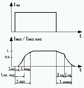
Fig. 5. To the definition of impulse parameters of optocouplers
Using this mixed design and schematic classification principle, it is logical to distinguish three main groups of optronic products: optocouplers (elementary optocouplers), optoelectronic (optronic) integrated circuits and special types of optocouplers. Each of these groups includes a large number of types of instruments.
For the most common optocouplers the following abbreviations are used: D - diode, T - transistor, R - resistor, U - thyristor, T2 - with composite phototransistor, DT - diode-transistor, 2D (2T) - diode (transistor) differential.
The system of parameters of optronic devices is based on the optocoupler parameters system, which is formed from four groups of parameters and modes.
The first group describes the input circuit of the optocoupler (input parameters), the second - its output circuit (output parameters), the third - combines the parameters characterizing the degree of exposure of the emitter to the photodetector and the associated features of the signal passing through the optocoupler as a coupler (parameters of the transfer characteristic) Finally, the fourth group combines galvanic isolation parameters, the values of which show how close the optocoupler is to the ideal decoupling element. Of the four listed groups, the parameters of the transfer characteristic and the parameters of the galvanic isolation are the defining, specifically "optocouplers".
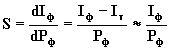
The most important parameter of the diode and transistor optocouplers is the current transmission coefficient. Determination of the impulse parameters of optocouplers is clear from (Fig. 5). The reference levels for measuring the parameters tpp (cp) , tcd , and t on (off) are usually the levels 0.1 and 0.9, the total time of the logical delay of the signal is determined by the level 0.5 of the pulse amplitude.
Parameters of galvanic isolation. Optocouplers are: the maximum permissible peak voltage between the input and output U of the raz n max ; Maximum permissible voltage between input and output U times max ; Resistance of galvanic isolation R ravel; Throughput capacity C razv; The maximum permissible voltage variation rate between the input in the output (dU razv / dt) max . The most important parameter is the U parameter, n max . It is he who determines the electrical strength of the optocoupler and its capabilities as an element of galvanic isolation.
The considered parameters of the optocouplers are used completely or with some modifications for the description of optoelectronic integrated circuits.
Diode Optocouplers
Fig. 6. Symbols of optocouplers
Diode optocouplers (Figure 6, a), to a greater extent than any: other devices, characterize the level of optocouplers. By the value of K i, one can judge the achieved efficiency of energy conversion in an optocoupler; The values of time parameters allow to determine the limiting rates of information dissemination. Connecting to a diode optocoupler of various amplifying elements, which is very useful and convenient, can not nevertheless give a gain either in energy or in limiting frequencies.
Transistor and thyristor optocouplers
Transistor optocouplers (Figure 6, c) have a number of properties that differ from other types of optocouplers. This is primarily a circuit-based flexibility, manifested in the fact that the collector current can be controlled both along the LED circuit (optically) and the base circuit (electrically), and also because the output circuit can work in both linear and key mode. The mechanism of internal amplification provides obtaining large values of the current transfer coefficient K i , so that subsequent amplifying stages are not always necessary. It is important that the inertia of the optocoupler is not very high, and for many cases it is quite acceptable. Output currents of phototransistors are much higher than, for example, photodiodes, which makes them suitable for switching a wide range of electrical circuits. Finally, it should be noted that all this is achieved with the relative technological simplicity of the transistor optocouplers.
Thyristor optocouplers (Figure 6, b) are most promising for switching high-current high-voltage circuits: by combining the power switched in the load and the speed they are clearly preferable to the T 2 -optopar. Optocouplers type AOU103 are designed for use as contactless key elements in various electronic circuits: in control circuits, power amplifiers, pulse formers, etc.
Resistor optocouplers
Resistor optocouplers (Figure 6, d) are fundamentally different from all other types of optocouplers by physical and structural-technological features, as well as the composition and values of the parameters.
The principle of the photoresistor's action is based on the effect of photoconductivity, that is, the change in the resistance of a semiconductor under illumination.
Differential optocouplers for analog signal transmission
All of the above material concerns the transmission of digital information on a galvanically isolated circuit. In all cases, when it was spoken about linearity, about analog signals, it was a question of the type of output characteristic of an optocoupler. In all cases, the control over the emitter-photodetector channel was not described by a linear dependence. An important task is the transmission of analog information by means of an optocoupler, that is, ensuring the linearity of the input-output transfer characteristic [36]. Only in the presence of such optocouples it becomes possible to directly distribute analog information over galvanically isolated circuits without converting it to a digital form (pulse train).
Comparison of the properties of different optocouplers with respect to parameters important from the point of view of the transmission of analog signals leads to the conclusion that, if this task can be solved, it is only with the help of diode optocouplers with good frequency and noise characteristics. The complexity of the problem lies primarily in a narrow range of linearity of the transfer characteristic and the degree of this linearity in diode optocouplers.
It should be noted that only the first steps have been taken to create devices with galvanic isolation suitable for the transmission of analog signals, and further progress can be expected.
Optoelectronic microcircuits and other devices of optron type
Optoelectronic microcircuits are one of the most widely used, developing, promising classes of optronic devices. This is due to the complete electrical and structural compatibility of optoelectronic chips with traditional microcircuits, as well as their wider functionality compared with elementary optocouplers. As with conventional microcircuits, switch optoelectronic microcircuits are most widely used.
Special types of optocouplers differ sharply from traditional optocouplers and optoelectronic microcircuits. These include, first of all, optocouplers with an open optical channel. In the design of these devices, there is an air gap between the emitter and the photodetector, so that by placing some mechanical obstacles in it, it is possible to control the light flux and thereby the output signal of the optocoupler. Thus, optocouplers with an open optical channel act as optoelectronic sensors that detect the presence (or absence) of objects, the state of their surface, the speed of movement or rotation, and so on.
Spheres of application of optocouplers and optocouplers
Prospective directions of the development and application of optronic technology have largely been determined. Optocouplers and optocouplers are effectively used to transfer information between devices that do not have closed electrical connections. Traditionally, the positions of optoelectronic devices remain in the technique of obtaining and displaying information. Independent optoelectronic sensors are designed to control processes and objects that are very different in nature and purpose. Significantly progressing functional optronic microcircuitry, focused on the implementation of a variety of operations associated with the transformation, storage and storage of information. Effective and useful is the replacement of cumbersome, short-lived and non-technological (from the position of microelectronics) electromechanical products (transformers, potentiometers, relays) optoelectronic devices and devices. Sufficiently specific, but in many cases justified and useful is the use of optocouplers for energy purposes.
Transfer of information
When transmitting information, optocouplers are used as communication elements, and, as a rule, do not carry an independent functional load. Their use makes it possible to carry out a very effective galvanic isolation of control and load devices (Fig. 7) operating under different electrical conditions and regimes. With the introduction of optocouplers, the noise immunity of communication channels increases sharply; Practically "parasitic" interactions on chains of "ground" and a feed are eliminated. Of interest is also the rational and reliable matching of digital integrated devices with a heterogeneous element base (TTL, ESL, I2L, CMOS, etc.).
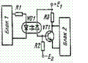
Fig. 7. Diagram of interblock galvanic isolation
The matching circuit of an element of transistor-transistor logic (TTL) with an integrated device on MIS-transistors is built on a transistor optocoupler (Fig. 8). In the specific version: E 1 = E 2 = 5 V, E 3 = 15 V, R 1 = 820 Ω, R 2 = 24 kOhm - the optocoupler LED is excited by a current (5 mA) sufficient to saturate the transistor and confidently control the device on the MOS Transistors.
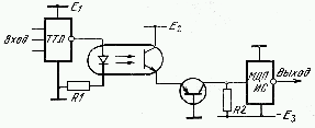
Fig. 8. Coupling scheme for TTL and MDS elements along an optical channel
Optical communications in telephone devices and systems are actively used. With the help of optocouplers, technically uncomplicated means can connect microelectronic devices intended for calling, indication, monitoring and other purposes to telephone lines.
The introduction of optical links into the electronic measuring equipment, in addition to the galvanic isolation of the object and the measuring instrument, which is useful in many respects, also makes it possible to drastically reduce the influence of interference acting along the ground and power circuits.
Of considerable interest are the possibilities and experience of using optoelectronic devices and devices in biomedical equipment. Optocouplers can reliably isolate the patient from the action of high voltages, available, for example, in electrocardiographs.
Noncontact control of high-power, high-voltage circuits through optical channels is very convenient and safe in complex technical conditions, typical for many devices and industrial electronics complexes. In this region, the positions of thyristor optocouplers are strong (Fig. 9).
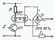
Fig. 9. AC load switching circuit
Obtaining and displaying information
Optocouplers and optocouplers occupy strong positions in the contactless remote technique of operative acquisition and accurate display of information about the characteristics and properties of very different processes and objects (by nature and purpose). Optocouplers with open optical channels possess unique capabilities in this respect. Among them, optoelectronic interrupters reacting to the intersection of an optical channel with opaque objects (Figure 10), and reflective optocouplers, in which the effect of light emitters on photodetectors is entirely related to the reflection of the radiated flux from external objects.
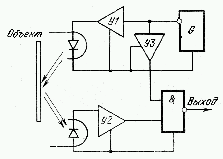
Fig. 10. Optoelectronic sensor
The range of applications of optocouplers with open optical channels is extensive and varied. Already in the 1960s, optocouplers of this type were effectively used to register objects and objects. With such a registration, which is characteristic primarily of devices for automatic monitoring and counting of objects, as well as for the detection and indication of various kinds of defects and failures, it is important to clearly locate the object or reflect the fact of its existence. The registration functions of the optocouplers are reliable and operative.
Control of electrical processes
The power of the radiation generated by the LED and the level of photocurrent arising in linear circuits with photodetectors are directly proportional to the current of the electrical conductivity of the radiator. Thus, by optical (contactless, remote) channels, it is possible to obtain quite definite information about the processes in electrical circuits galvanically connected with the radiator. Especially effective is the use of light emitters of optocouplers as sensors of electrical changes in high-current, high-voltage circuits. Clear information on such changes is important for the operational protection of energy sources and consumers from electrical overloads.
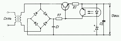
Fig. 11. Voltage stabilizer with control optocoupler
Optocouplers operate successfully in high voltage voltage regulators, where they create optical channels of negative feedbacks. The stabilizer under consideration (Fig. 11) refers to a serial device, with the bipolar transistor being the regulating element, and the silicon zener diode acts as a source of reference (reference) voltage. The comparative element is the LED.
If the output voltage in the circuit of Fig. 11 increases, the conduction current of the LED also increases. The phototransistor of the optocoupler acts on the transistor, suppressing the possible instability of the output voltage.
Replacement of electromechanical products
In the complex of technical solutions aimed at increasing the efficiency and quality of automation, radio engineering, telecommunications, industrial and consumer electronics devices, it is expedient and useful to replace electromechanical products (transformers, relays, potentiometers, rheostats, pushbuttons and key switches) with more compact, High-speed analogues. The leading role in this direction is assigned to optoelectronic devices and devices. The fact is that very important technical advantages of transformers and electromagnetic relays (galvanic isolation of control and load circuits, reliable operation in high-power, high-voltage, high-current systems) are also characteristic of optocouplers. At the same time, optoelectronic products significantly exceed the electromagnetic counterparts for reliability, durability, transient and frequency characteristics. Control of compact and high-speed optoelectronic transformers, switches, relays is carried out with the help of integrated microcircuits of digital technology without special means of electrical matching.
An example of replacement of a pulse transformer is shown in Fig. 12.
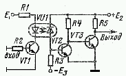
Fig. 12. Scheme of optoelectronic transformer
Energy functions
In the power mode, optocouplers are used as secondary sources of EMF and current. The efficiency of optocouplers is small. However, the possibility of introducing an additional voltage or current source into any circuit of the device without galvanic coupling with the primary power source gives the developer a new degree of freedom, especially useful in solving non-standard technical problems.

Comments
Commenting on, remember that the content and tone of your message can hurt the feelings of real people, show respect and tolerance to your interlocutors even if you do not share their opinion, your behavior in the conditions of freedom of expression and anonymity provided by the Internet, changes Not only virtual, but also the real world. All comments are hidden from the index, spam is controlled.