
|
Start of section
Production, amateur Radio amateurs Aircraft model, rocket-model Useful, entertaining |
Stealth Master
Electronics Physics Technologies Inventions |
Secrets of the cosmos
Secrets of the Earth Secrets of the Ocean Tricks Map of section |
  |
| Use of the site materials is allowed subject to the link (for websites - hyperlinks) | |||
Navigation: => |
Home / Electronics / Schemes / Power supply of equipment / |
|
THE DIAGRAM OF THE OPERATED STABILIZER OF THE NETWORK VOLTAGE
Author of the article: Sergey Abramov
The proposed network voltage regulator circuit differs from the previously described ones in that the voltage feedback is organized using an optocoupler. Due to the inertia of the light bulb in the OEP2 optocoupler, some hysteresis is achieved, which is mandatory in feedback circuits. Without hysteresis there will be a relaxation of the circuit which will be expressed in the blinking of the HL1 light bulb, which is a load in this circuit.
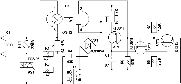
Consider the operation of the circuit depicted in Figure 1 . When the mains voltage is turned on, the sinusoidal voltage limited by the resistor R4 is applied to the diode bridge VD1 . On the load voltage is absent, therefore, the resistance of the optocoupler is large, the transistor VT1 is opened due to the displacement coming from the resistor R6 . The current flowing through the resistor R5 and the open transistor VT1 charges the capacitance C1 . At the moment when the voltage reaches the level of the breakdown of the analog of the dynistor, the capacitor C1 accumulated on the parts VT2, VT3, R7, R8 is discharged into the primary winding of the pulse transformer T1 . As a result, a pulse from the secondary winding will be opened by a triac VS1 . The time for the charging rate of the capacitor and, hence, the opening time of the triac depends on the resistance R5 and the resistance of the emitter-collector transition of the transistor VT1 .
By closing this transistor, we reduce the voltage on the load, which is what happens, due to the decrease in the resistance of the resistor of the optocoupler. The threshold on which the balance comes is regulated by resistor R2 , which is behind the output voltage sensor.
Setting is to set the maximum voltage with the help of resistor R5 with the wire disconnected from potentiometer R2 and optocoupler U1 .
Details the transformer T1 is wound on the ferrite ring M2000NM in size K20x12x6 . The primary winding consists of 100 turns, and the secondary winding consists of 60 turns of PEV1 wire with a diameter of 0.15 mm .
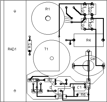
The device is assembled on a single-sided PCB with a size of 70x70 mm . Shown in Fig. 2 .
print version
Author: Abramov Sergey, Orenburg
PS The material is protected.
![]()

Comments
When commenting on, remember that the content and tone of your message can hurt the feelings of real people, show respect and tolerance to your interlocutors even if you do not share their opinion, your behavior in the conditions of freedom of expression and anonymity provided by the Internet, changes Not only virtual, but also the real world. All comments are hidden from the index, spam is controlled.