| section Home
Production, Amateur Radio amateur Model aircraft, rocket- Useful, entertaining |
Stealth master
Electronics Physics Technologies invention |
space Mystery
Earth Mysteries Secrets of the Ocean Stealth section Map |
  |
| Use of material is permitted for reference (for websites - hyperlinks) | |||
Navigation: => |
Home / Inventions / Alternative Energy / |
|
Semiconductor converters THERMAL ENERGY ENVIRONMENT
The ENERGY direct electric current
Authors: Anatoly grain
The problem of modern power consists in the fact that the production of electricity - a source of human material wealth, is in ruinous confrontation with its habitat - the nature and as a result of this - the inevitability of environmental disaster.
Search and discovery of alternative, cleaner ways to produce electricity - the actual task of Humanity.
One of the sources of energy, is a natural environment: the air of the atmosphere, water, seas and oceans, which contain an enormous amount of heat energy from the sun.
A method for converting thermal energy of the environment into the energy of a constant electric current, based on the phenomena of contact between the metal and semiconductors of different conductivity type.
Results: a schematic diagram of the inverter, the technological conditions of production and a brief description of the operating principle.
Converter is a schematic diagram of the following (see. Fig. 1).
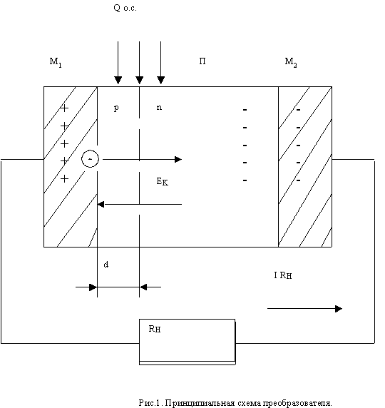
where: P - the semiconductor chip (silicon n-type); p-n - the transition from the contact electric field Ek; M 1 - metallic contact with the p-region (aluminum); M 2 - metal contact with n-region (aluminum); d - depth of the p-n junction (no more than 10 microns); RH - load resistance of the external circuit.
The principle of operation of the converter is as follows.
For example, the work function of the n-type semiconductor is 4.25 eV, a p-type - 5.25 eV Aluminum - 4.25 eV. Therefore, contact M 2 with n-type semiconductor is ohmic and does not affect the operation of the converter and the contact M 1 with a p-type semiconductor is injecting.
Under the influence of thermal motion and forces resulting from the difference of work function, electrons from the metal contact M 1 are injected into the p-semiconductor. Some of the electrons recombine with holes in the p-region of the crystal, and the rest of the electrons will be shifted electric field of p-n transition Ek in the n-region of the crystal. In this n-crystal semiconductor region and the contact M 2 are negatively charged and terminal M 1 of the departure from it electrons - positive, which ultimately lead to the emergence of the electrical potential difference between the terminals of M 1 and M 2.
The flow of electrons in M 1 M 2 takes place as long as the increasing electric field between the counter-contacts does not cause the flow of electrons from the n-p-region in the crystal region due to lower the potential barrier of p-n junction. When the electron currents become equal, install electrical and thermodynamic equilibrium in an isolated crystal. At the same time contacts between M 1 and M 2 is established a potential difference equal to half the difference between the contact potential of the pn junction (in this case - 0,55V), which means that between EMF (idle move).
If close contact M 1 and M 2 external metallic conductor with a resistance RL, the electrical and thermodynamic equilibrium of the semiconductor crystal and disturbed flow in the load circuit electric current I RL. This pn junction will be cooled, t. To. The energy of the electrons passing from the p-type region to the n-semiconductor region will be increased due to the internal (thermal) energy of the crystal lattice of a semiconductor. To maintain a constant load circuit by a current value necessary to supply to the crystal heat from the environment - Qo. c.
print version
Author: Anatoly grain
PS material is protected.
Publication date 04.04.2004gg
![]()

Comments
Commenting, keep in mind that the content and the tone of your messages can hurt the feelings of real people, show respect and tolerance to his interlocutors, even if you do not share their opinion, your behavior in terms of freedom of speech and anonymity offered by the Internet, is changing not only virtual, but real world. All comments are hidden from the index, spam control.