| section Home
Production, Amateur Radio amateur Model aircraft, rocket- Useful, entertaining |
Stealth master
Electronics Physics Technologies invention |
space Mystery
Earth Mysteries Secrets of the Ocean Stealth section Map |
  |
| Use of material is permitted for reference (for websites - hyperlinks) | |||
Navigation: => |
Home / Products Patents / In the section of the catalog / back / |
|
INVENTION
Russian Federation Patent RU2170994
![]()
METHOD FOR PRODUCING SOLID photovoltaic cells for converting the energy of light in electrical energy
Name of the inventor: Fedorov MI .; Smirnova MN .; SV Karelin
The name of the patentee: Vologda State Technical University
Address for correspondence: 160035, Vologda, ul. Lenin 15, Vogt Patent Department
Starting date of the patent: 2000.04.05
The invention relates to optoelectronics, in particular to a device that converts radiant energy into electrical energy, and can be used in semiconductor electronics, in particular optoelectronics and in medical technology with UV irradiation in fiziokabinet on APC plants when irradiated animals environmental low measurement intensities of radiation from TV screens and computer monitors. The technical result of the invention is to improve the sensitivity of the photo-emf. Summary of the invention: the substrate of the inorganic semiconductor is gallium arsenide (GaAs), heavily doped with donor impurities, is applied by vacuum deposition of a thin organic semiconductor layer of n-type hlorindiyftalotsianina (ClInPc), having a high absorption coefficient in the UV region. Production of solid-state solar cell proposed method allows to increase the photosensitivity of 10 -4 W / m 2.
DESCRIPTION OF THE INVENTION
The invention relates to optoelectronics, in particular to a device that converts radiant energy into electrical energy, and can be used in devices for measuring the illumination intensity of the radiation dose of UV irradiation in the agricultural sector and as a sensor for determining the concentration of ozone layer of the Earth.
A method for manufacturing a thin-film photoelectric converter with a pin-structure based on ![]() = Si: H (US patent N 4772335, cl 136/258. 1988).
= Si: H (US patent N 4772335, cl 136/258. 1988).
This manufacturing method is as follows: a glass substrate coated ohmic back electrode. Electrode deposited on the thin layer of doped p- or n-type deposition ![]() = Si: H in the gas phase. On the doped layer is deposited from a gas phase deposition of a thick layer of undoped
= Si: H in the gas phase. On the doped layer is deposited from a gas phase deposition of a thick layer of undoped ![]() = Si: H. In undoped layer is deposited from a gaseous phase deposition a second layer of doped p- or n-type of
= Si: H. In undoped layer is deposited from a gaseous phase deposition a second layer of doped p- or n-type of ![]() = Si: H. The second doped layer
= Si: H. The second doped layer ![]() = Si: H is applied to the upper electrode as a conductive film of SnO 2. The upper electrode is applied to the metal collector. The upper electrode is placed quartz glass. Quartz glass coated with an antireflection coating of CaF 2 or MgF 2.
= Si: H is applied to the upper electrode as a conductive film of SnO 2. The upper electrode is applied to the metal collector. The upper electrode is placed quartz glass. Quartz glass coated with an antireflection coating of CaF 2 or MgF 2.
A photoelectric converter manufactured in this manner has a sensitivity in the Photovoltaic 200-400 nm. However, obtained by this method ultraviolet fotoelektriicheskih converters, there are significant drawbacks: the impossibility of obtaining the spectral photosensitivity in a wide range of 200 - 1000 nm, the inability to obtain a high photosensitivity by a photo-emf measuring low intensity, complexity of manufacturing technology.
A method for manufacturing a solid-state solar cell for converting light energy into electrical energy (. RF patent N 2071148, cl H 01 L 31/18, 1996), which is as follows: gallium arsenide on a plate of 0.4 mm thick previously subjected to etching, is applied rear ohmic electrode of an alloy of germanium and gold. On the opposite surface of gallium arsenide deposited in vacuo photosensitive layer of copper phthalocyanine 20 nm thick. Copper phthalocyanine layer is subjected to doping of purified oxygen. Phthalocyanine sprayed layer on the translucent electrode made of silver, which transmits 10% of incident light. The disadvantage of this method is low photosensitivity of the photo-emf.
The purpose of the present invention - increase the photosensitivity of photo-emf.
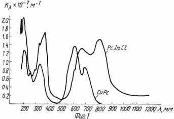
For this purpose, the method for producing ultraviolet converter comprising applying to the semiconductor substrate of the photosensitive layer, its doping and coating the opposite side of the electrodes, as a substrate material using an inorganic semiconductor gallium arsenide (GaAs), heavily doped with donor impurities, and the photosensitive layer is applied by vacuum deposition of organic n-type semiconductor hlorindiyftalotsianina (ClInPc), having a high absorption coefficient and high photosensitivity in the UV region (FIG. 1).
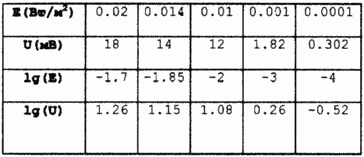
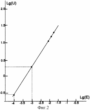
The new proposed method compared to the prior art is to apply the photosensitive layer hlorindiyftalotsianina (ClInPc) on a substrate of gallium arsenide (GaAs), thus improving the photosensitivity to 10 -4 W / m 2 (FIG. 2).
BRIEF DESCRIPTION graphical pictures, where FIG. 1 - absorption spectrum of the CuPc and ClInPc; FIG. 2 - U dependence idling voltage E of irradiation intensity on a logarithmic scale, constructed on the basis of experimental data given in the table.
 |
 |
 |
Example: on the plate of gallium arsenide heavily doped with donor impurities, 0.4 mm thick, pre-etched, causing the rear ohmic electrode of an alloy of germanium and gold. On the opposite surface of gallium arsenide deposited in vacuo photosensitive layer of an organic n-type semiconductor hlorindiyftalotsianina (ClInPc) 20 nm thick. Hlorindiyftalotsianina layer subjected to doping purified oxygen. Hlorindiyftalotsianina sprayed layer on the translucent electrode made of silver, which transmits 10% of incident light. Production of solid-state solar cell proposed method improves fotochuvstvitlnost to 10 -4 W / m 2. |
CLAIM
A method of manufacturing a solid-state solar cell for converting light energy into electrical energy comprising applying an organic photosensitive layer on a semiconductor substrate of an inorganic semiconductor and placing them between two electrodes, one of which is translucent, characterized in that the inorganic semiconductor is used as the gallium arsenide n- type (n + -GaAs), as well as organic semiconductor thin layer hlorindiyftalotsianina n-type (n-ClInPc).
print version
Publication date 12.01.2007gg
![]()

Comments
Commenting, keep in mind that the content and the tone of your messages can hurt the feelings of real people, show respect and tolerance to his interlocutors, even if you do not share their opinion, your behavior in terms of freedom of speech and anonymity offered by the Internet, is changing not only virtual, but real world. All comments are hidden from the index, spam control.