
| Start of section
Production, amateur Radio amateurs Aircraft model, rocket-model Useful, entertaining |
Stealth Master
Electronics Physics Technologies Inventions |
Secrets of the cosmos
Secrets of the Earth Secrets of the Ocean Tricks Map of section |
  |
| Use of the site materials is allowed subject to the link (for websites - hyperlinks) | |||
Navigation: => |
Home / Patent catalog / Catalog section / Back / |
|
INVENTION
Patent of the Russian Federation RU2242064
![]()
SOLAR ELEMENT
The name of the inventor: Gippius AA (RU); Enisherlova-Vel'yasheva K.L. (RU); Konstantinov P.B. (RU); Kontsevoy Yu.A. (RU)
The name of the patent owner:
PN Lebedev of the Russian Academy of Sciences
Address for correspondence: 119991, Moscow, B-333, GSP-1, Leninsky Prospect, 53, FIAN them. P.N. Lebedev, the patent department
Date of commencement of the patent: 2003.07.16
The invention relates to the construction of solar cells. Essence: the design of a solar cell containing a base region of a single conductivity type, preferably 30-170 μm in thickness, a pn junction and a contact comb on the front side, and a heavily doped layer of the same type as the base, such as conductivity and ohmic contact on the back side , The heavily doped layer on the rear side being connected to a grate made of silicon, and the ohmic contact on the rear side is connected to the grate and heavily doped layer. In addition, the base region and the grating are proposed to be made on the basis of plates with different crystallographic orientations. In particular, the base region can be formed on a silicon orientation plate (111), and the lattice is formed on the basis of silicon orientation plates (100). The technical result of the invention is the increase in the strength of solar cells.
DESCRIPTION OF THE INVENTION
Solar cells are the main elements of solar cells, widely used as sources of electrical equipment for spacecraft and satellites.
Solar cells based on p-type silicon with a pn junction and a contact comb on the front side and an ohmic contact on the back side are known / 1 /. The disadvantage of such solar cells is low efficiency because of the increased rate of surface recombination at the back ohmic contact.
A solar cell based on a p-type silicon wafer containing a pn junction and a comb on the front side and a heavily doped region on the underside of the plate are known to reduce the surface recombination rate (1). However, such an element with a thickness of the base region of the hole conductivity of 200 μm or more is subject to degradation under the influence of radiation existing in space, due to the reduction of the diffusion length / 1 /. A more radiation-resistant solar cell should have a thickness of the base region of the hole conductivity of 100 μm or less.
As a prototype, a thin solar cell having a base region thickness in the range of 30-170 μm / 2 / is chosen. Prototypes used to protect the solar cell from mechanical damage were layers of polymer 10-30 μm in thickness. However, such a solar cell still has inadequate mechanical strength, which complicates thermocycling when the satellite moves from the illuminated zone to the Earth's shadow. In addition, the installation of solar cells of small thickness is associated with a decrease in the yield percentage due to the reduced strength of solar cells.
The object of the invention is to increase the strength of solar cells.
The problem is solved as follows. A solar cell containing a base region of one conductivity type, preferably 30-170 μm in thickness, a pn junction and a contact junction on the front side, and both the heavily doped layer and the ohmic contact on the rear side are connected by a heavily doped layer with a grate made of silicon, and the ohmic contact On the rear side is connected with a lattice and a heavily doped layer.
In addition, the base region and the grate are made on the basis of plates with different crystallographic orientations. In particular, the base region can be formulated on a silicon orientation plate (111), and the lattice is formed on the basis of the silicon orientation plate (100), which greatly increases the strength of the solar cell, since its parts do not have common fault planes.
 |
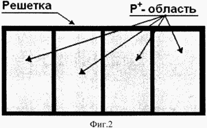 |
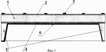
FIG. 1 is a sectional view of a solar cell structure according to the present invention. FIG. Here (1) is the base region (of hole conduction); (2) is the pn junction; (3) - the contact comb on the front side of the solar cell; (4) - heavily doped region (P + -type) on the back side of the base region; (5) is a silicon lattice bonded to a heavily doped layer on the back side of the base region; (6) is the ohmic contact associated with the heavily doped layer on the back side of the base region and with the silicon lattice (5).
2 shows the design of the solar cell (rear view).
This solar cell has dimensions of 50 × 25 mm. The width of the sides of the grid (shown in dark color) for different options is 0.5-1.0 mm, thickness is 300 μm.
The solar cell works as follows. When illuminated from the front side, nonequilibrium charge carriers arise, which diffuse through the base region 1, separated by pn by the junction 2, and the operating current is created. The current of the holes moving to the ohmic contact passes through the P + layer 4 to the metallic ohmic contact 6. Thus, a closed circuit for the current is created.
The models of solar cells were created, according to the description of this application, with a minimum thickness of the base region of 30 μm. Investigation of the properties of solar cells showed that solar cells have sufficient mechanical strength, determined by the thickness of the lattice, and withstands repeated cycles from the temperature of liquid nitrogen to 100 degrees Celsius.
USED BOOKS
1. SMSze. Physics of Semiconductor Devices. John Wiley & Sons. New York. 1981. Ch.14 (S.Z., Physics of Semiconductor Devices, Translated from English / Edited by R. A. Suris, in 2 books, book 2, Ch.14).
2. Pat. USA 5650363, Jul. 22, 1998.
CLAIM
1. A solar cell comprising a base region of one conductivity type, preferably 30-170 μm in thickness, a pn junction and a contact junction on the front side, and a heavily doped layer of the same base as the conductivity type and an ohmic contact on the rear side, , That the heavily doped layer on the rear side is connected to a grate made of silicon, and ohmic contact from the rear side is connected to the grate and heavily doped layer.
2. Solar cell according to claim 1, characterized in that the base region of the solar cell and the silicon lattice have a different crystallographic orientation.
3. A solar cell according to claim 1 or 2, characterized in that the base region has a crystallographic orientation (111), and the silicon lattice has a crystallographic orientation (100).
print version
Date of publication 12.01.2007gg
![]()

Comments
When commenting on, remember that the content and tone of your message can hurt the feelings of real people, show respect and tolerance to your interlocutors even if you do not share their opinion, your behavior in the conditions of freedom of expression and anonymity provided by the Internet, changes Not only virtual, but also the real world. All comments are hidden from the index, spam is controlled.