| section Home
Production, Amateur Radio amateur Model aircraft, rocket- Useful, entertaining |
Stealth master
Electronics Physics Technologies invention |
space Mystery
Earth Mysteries Secrets of the Ocean Stealth section Map |
  |
| Use of material is permitted for reference (for websites - hyperlinks) | |||
Navigation: => |
Home / Products Patents / In the section of the catalog / back / |
|
INVENTION
Russian Federation Patent RU2027217
![]()
SECONDARY POWER SUPPLY
Name of the inventor: Greenberg GM .; Mizrakh EA .; Petunin VM .; Petrakov EV
The name of the patentee: Siberian Aerospace Academy
Address for correspondence:
Starting date of the patent: 1991.01.03
Usage: to simulate the current-voltage characteristics (CVC) of primary energy sources, in particular solar. The inventive improves fidelity source required CVC, namely eliminates errors CVC play caused by the failure of transforming cells (IL). N source consists of feed channels (PC) are connected in parallel between the input and output terminals. The first PC includes AEs shunt transistor (PCS) and the decoupling diode (RD). The second computer includes IL, PCS, RD, two comparators and a switch (P), and the rest of the PC added adder. To reproduce the desired IVC M PC used, the first PC provides linear control of its output current (BT) and from the second computer to M-th provide discrete control of its total TSR. The remaining (NM) PC is used as a backup. Selecting the main or backup PC mode implemented via AP In case of failure of one or more AEs replace faulty PCs connected corresponding number of PCs among the reserve. To eliminate redundant connection in case the PC normal operation basic PC comparators are combined by the output of the logic OR.
DESCRIPTION OF THE INVENTION
The invention relates to electrical engineering and can be used to simulate the current-voltage characteristics (CVC) of primary energy sources, in particular solar.
Known secondary power supply, with a special form of the CVC [1], used as a solar simulator, consisting of a series of converter cells - current regulators, connected at the input to the power supply pins for U n, and to overcome through decoupling diodes to the load. The outputs of converter cells are shunted transistors, the base terminal of the transistor is connected to the output of the comparison unit, to the input terminals of which are connected voltage reference, power output and current sensor included in the load circuit. Base terminals through transistors remaining comparators connected to the output load current sensor.
The disadvantages of such a source is the low reliability and fidelity required CVC due to the cycle of the output currents converting cell values and thresholds triggering comparators.
Known and the secondary power source [2] containing N cells - current regulators connected inputs with terminals for connecting the supply voltage source, the load current sensor, a reference voltage comparison unit with a total voltage value of the sensor current and the output voltage, N transistors, N decoupling diodes, N-1 and N-comparators and two adders.
A drawback of this secondary power source is a low fidelity required IVC due offset coordinates steep portion IVC in case of failure of the cell - current regulator of any of the feed channels or due to the fact that in the case of the first feed channel failure cell isolation the diode is closed and a linear regulator is disconnected from the output terminals of the source.
The purpose of the invention - improved accuracy CVC play.
The objective is achieved in that the secondary power supply comprising N cells - stabilizers AC coupled input with terminals for the power supply voltage, the load current sensor, the comparison unit a reference voltage from the total voltage value of the sensor current and the output voltage, N transistors, N decoupling diode, N-1 comparators, where the collector-emitter circuit of the transistors, except the first, is connected across the output of the respective cells - current regulators, the first transistor base connected to the output of the comparison unit and the base remaining transistors are connected to the outputs of respective basic comparators cell outputs - stabilizers current through the respective decoupling diodes are connected to a terminal for connecting load cells - current stabilizers in all feed channels other than N-th, equipped with data outputs, as the reference voltage of the second feed channel used data output cell - current regulator of the first supply channel, a reference voltage source subsequent feed channels are in the form of adders, wherein each adder inputs i-th feeding conduit connected to the ground reference input of the comparator and information output cell - current stabilizer (i-1) -th supply channel introduced komparatopov N-1, N-1 switches and a reference voltage source, wherein the reference inputs of additional comparators are connected to a further voltage reference, in all feed channels of the outputs of the main and additional komparatopov connected to each other, a signal input of additional comparators all feed channels connected to the switching contact of its switch feeding conduit normally closed contact which is connected to the common bus, and NO - to the reference input of the comparator their main supply channel, moreover, in the first cell output feed channel - the current stabilizer circuit connected with the collector-emitter transistor via a decoupling diode.
Comparative analysis of the inventive solution and prior art shows that first introduced additional N-1 comparators, N-1 switches, but also a reference voltage source, wherein the reference inputs of additional comparators are connected to a further voltage reference, in all feed channels of the outputs of the main and auxiliary comparators connected to each other, a signal input of additional comparators all feed channels connected to the changeover contact switch its supply channel, break contact of which is connected to the common bus, and NO - to the reference input of the basic comparator their feed channel, in addition, the first feed channel cell output - current regulator is connected to the collector-emitter circuit of the transistor via a decoupling diode. Thus, the claimed technical solution meets the criterion of "novelty".
The collection known and introduced elements and their relationship caused a new property if to form a steep section of the source of the CVC is required number of feed channels M, less the total amount of feed channels N, the remaining S = NM feed channels can be used as back-up connected to the output of the source instead of the failed main feed channels. In case of failure of the cell - the first current regulator in the supply channel closes decoupling diode which disconnects the defective cell - Stabilizer output current from the source. A linear regulator is not disabled and provides the desired change in the source of the CVC. As a result, excluded mode when shifting the coordinates of the source CVC steep section of the point I n = M · I, I, as the number of M workers feed channels is maintained constant, and the regime as a linear regulator is disconnected from the output terminals of the source, the output voltage of the source is not regulated and it is determined by the output voltage of the healthy feeding channels.
Thus, the claimed source is provided to achieve a positive effect, is to improve the fidelity required by CVC to eliminate bias current position I n steep section from M · I I elimination mode, when there is a change in the unregulated output voltage source. This allows to conclude that the proposed technical solution the criterion of "substantial differences".
The drawing is a block diagram of the inventive power source.
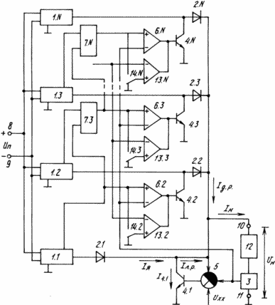 |
Secondary power supply contains 1.1-1.N cell - pulse current stabilizers, fitted with data outputs (with individual current sensors), decoupling diodes 2.1-2.N, sensor 3 of the load current, transistors 4.1-4. N and comparing unit 5. In the first feeding channel comparators 6.1, 13.1 and 14.1 of the switch is not used, and in other supply channels used comparators 6.2-6.N, 13.2-13.N 14.2-14.N and switches. In the first and second feeding channels installation adders 7.1 and 7.2 is not necessary, and the rest of the feed channels introduced 7.3-7.N adder. The diagram marked and conclusions of 8 and 9 for the connection of the primary power source terminals 10 and 11 to connect the load 12 and the voltage reference U xx and U ON. Reference input in 6.2-6.N comparators and signal input into the comparators 13.2-13. N are inventipuyuschimi, the signal input to the comparators. 6.2-6.N and reference input to comparator 13.2-13. N - inverts. Comparators 6.2-6. N and 13.2-13.N pairs are combined and their output signals are combined in the overall yield of the logic OR. In 521SA1 chip (VL Shilo Linear integrated circuits in electronic equipment. M .: Soviet Radio, 1979, pp. 220-221) can be used as a pooled comparators. |
1.1-1.N cells are connected in parallel via the decoupling diode and sensor 3 2.1-2.N load current between terminals 8 and 9 for the connection of the primary power source and the terminal 10 and 11 to connect the load. Outputs cells 1.1-1.N shunted transistors 4.1-4.N. The comparison unit 5 inputs connected to the outputs of the reference voltage U xx sensor 3 of the load current and the total potential output of the source (after decoupling diodes 2.1-2 N.), And the output - to the base of the transistor circuit 4.1.
Signal inputs of comparators 6.2-6. N connected to the output load current sensor 3. The combined reference input of the comparator 6.2 and 14.2 make contact switch connected to the data input of the cell 1.1, and the combined reference input of each comparator 6.i and make contact 14.i each switch of the plurality of the other comparators and switches through 7.i adder connected to the reference input of the comparator 6. (i-1) and the data output of the cell 1. (i-1).
The reference inputs of comparators 13.2-13.N combined and connected to the source of the reference voltage U op. Signal inputs 13.2-13.N comparators are connected to the switching contacts 14.2-14.N switches NC contacts are connected to a common bus. The outputs of comparators 6.2-6.N and 13.2-13.N are interconnected and connected to the respective base circuits of transistors 4.2-4.N.
POWER WORKS AS FOLLOWS
When applying an input voltage U n each 1.1-1.N cells stabilizes its output current level I, I. Connecting 1.2-1.N cells to the load carried diode-transistor switches, consisting of a diode and 2.2-2.N 4.2-4.N transistors. Signal transistor Management 4.1 is fed from the output of the comparison unit 5, transistors 4.2-4.N - with outputs of comparators 6.2-6.N and 13.2-13.N. Depending on the state of the comparators 6.2-6. N and 13.2-13. N 4.2-4.N transistors are either in the open or closed state. Accordingly 1.2-1.N cell operates in either short-circuit mode when the currents in the load 12 is not received or the mode of energy transfer to the load.
A voltage proportional to the output currents 1.1-1.N cells are removed from the data outputs of these cells and fed to the inputs of adders 7.3-7. N. threshold comparator U v.i 6.i determined by the output voltage of the adder and 7.i proportional to the sum of the output currents of all previous cells:
U 6.i = (i-1) KI I, (1) where K - coefficient of proportionality.
Thresholds are 6.2-6.N comparators are in the ratio
U 6.2 <U 6.3 <... < U 6.N. (2)
Thresholds comparator trip 13.2-13.N determined voltage U op and are chosen within the
(M-1) I of I K <U op <(M) I of I K, (3) and the voltage U 13.i, applied to the signal inputs of comparators 13.2-13.N, defined by the expression
U 13.i = (i-1) I of I K> U OP, (4) if the signal inputs of the comparator switches through 14.2-14. N combined with the reference input of the comparator 6.2-6.N, or zero, if these inputs through switches 14.2-14.N shorted to a common bus.
The output of comparators 6.2-6.N to logic "1" if the voltage at its signal input is less than the voltage on the reference input, a logic "0" if the voltage at its signal input is equal to or greater than the voltage on the reference input. The output of comparators 13.2-13.N set logic "0" if their signal inputs via switches 14.2-14.N are connected to a common bus, if their input signal via switches 14.2-14. N are connected to the reference input of the comparator and voltage U 6.2-6.N 13.I on these inputs is less than U op. The output of the comparator is set 13.2-13.N logical "1" if their signal inputs through switches 14.2-14.N connected to the reference input of the comparator and voltage U 6.2-6.N 13.I on these inputs over U op.
The initial state of the circuit. The output of comparators 6.2-6.N voltage corresponds to a logical "1". Switching contacts are closed 14.2-14.M switches with NC contact and on the outputs of the comparators 13.2-13.M voltage corresponds to a logical "0". The switching contacts of the other switches 14. (M + 1) -14. (M + S) with normally open contacts are closed and at the outputs of the comparator 13. (M + 1) -13. (M + S) voltage corresponds to a logic "1". On the bases of transistors 4.2-4.N voltage corresponding to the logical "1" and transistors 4.2-4.N open.
As long as the load current I n <I I voltage U 3 at the output of the sensor 3 is less than the load current threshold comparator 6.2, all comparators 6.2-6.N, 13.2-13. N, 4.2-4.N transistors are in the initial state. The required output voltage of the power supply
U n = U xx - I of Mr. K 3 (5) provides a linear voltage regulator, consisting of a transistor cell 4.1 1.1 unit 5 and the comparison reference voltage U 3 K xx - transmission ratio sensor 3 of the load current.
In idle mode (I n = 0), the output power supply voltage U n = U xx. With the current rise I n transistor 4.1 is closed and according to the expression (5) voltage U n linearly decreases. When current I n = I 4.1 I transistor is closed, the load cell 12 receives all the output current of 1.1, equal to the voltage U n U xx - I and K 3, and the voltage at the output of the sensor 3, the load current reaches a threshold comparator 6.2.
When triggered, the voltage comparator on the basis of 6.2 4.2 voltage transistor becomes logic "0" and closes the transistor 4.2. 4.2 Closing the transistor causes an abrupt increase in load current I n, which leads to the opening of transistor 4.1 and reduction to zero of the output current I LR linear regulator. Output voltage U n and the output current I n are the source in this case equal respectively U xx -I and K 3 and I, I.
A further reduction of the load resistance R n and a corresponding increase in the current I n is accompanied by a linear reduction in voltage U N according to expression (5). When current I n = 2I I output voltage of the sensor 3 is equal to the load current operation threshold comparator 6.3. At this point, the base voltage of the transistor 4.3. voltage becomes logic "0". 4.3 A transistor is closed, the exit source connected cell 1.1-1.3 and the current I n increases abruptly to the value I 3I. Opens transistor 4.1, the current I n is reduced to the desired value 2I, I and voltage U n is equal to U xx -2I I K 3.
I n A further increase in the current causes alternating triggering comparators 6.4-6. M, closing transistors 4.4-4.M and connection to the output of the power supply 1.4-1.M cells. When a current I n is equal to (M-1) I I activated comparator 6. M 1.m cell recoil energy transferred to the load 12 mode, and increasing the current I to n · I value I M takes place by reducing the current I 4.1.
When current I n = MI I reached threshold comparator 6. (M + 1). But the state of the transistor 4 (M + 1) does not change, since the voltage at the output of the comparator 13. (M + 1) corresponds to a logical "1".
Thus, when the current I n = MI i to the output of 1.1-1 cells connected to the power supply. M, the current I is zero and 4.1 decrease in voltage U n a further reduction of the load resistance R n occurs at a constant current I n accordance with the expression
U n = R n · I MI
On the power supply output is generated approximate CVC solar coordinates: open circuit voltage U xx, short-circuit current of M · I I.
As the resistance R n and decreasing the current I n is a gradual shutdown 1.1-1.M cells from the exit of the secondary power source.
From this it follows that the current I LR adjusted so as to always satisfy the condition (5), and the change in current I DR It is made in such a way that the current I 4.1 does not exceed the value of I i.
In case of failure of one of the cells 1.1-1.M their total output current I to n decreases the output current I I of that cell. Operates power source in this case is as follows.
In case of failure, for example, cell 1.i its output current is equal to zero. The voltage at the signal input of the comparator 13. (M + 1) -13. (M + S) and the thresholds of comparators 6. (i + 1) -6.N thus reduced by an amount proportional to I i. Voltage U 13. (M + 1) at the signal input of the comparator 13. (M + 1) equal to the expression (4) M ![]() I and K, in this case reduced to a value of (M-1) · I K and I becomes smaller than the threshold of the comparator 13. The op U (M + 1) given by expression (3). The comparator 13 (M + 1) goes to the state when the voltage is set at its output corresponding to a logical "0".
I and K, in this case reduced to a value of (M-1) · I K and I becomes smaller than the threshold of the comparator 13. The op U (M + 1) given by expression (3). The comparator 13 (M + 1) goes to the state when the voltage is set at its output corresponding to a logical "0".
Upon reaching the current value I n (i-1) I I immediately triggered two comparators: 6. i and 6. (i + 1). Actuation 6.i comparator 4.i and closing of the transistor can not lead to a change in output current I dr Digital controller (1.i cell output current is zero, and when the comparator is triggered 6. (i + 1) and the closing of the transistor 4. (i + 1), the current I is increased by dr (i-1) to the value I iI iI.
Alternating actuation remaining comparators 6. (i + 2) and closing -6.M transistor 4. (i + 2) -4.M increases the current I dr to the value (M-2) I I, when connected to the output of the source of all the workers of the main cells 1.1-1. M represents a logical "0" In this case reached threshold comparator 6 (M + 1), and superposed on the voltage outputs of the comparators 6 (M + 1) and 13. (M + 1). 4. The transistor (M + 1) is closed, the exit is connected to the source of the backup cell 1. (M + 1) and the output current is increased to a discrete controller (M-1) I of myself.
Failure of two of the cells causing the change of state 1.1-1.M comparators 13. (M + 1) and 13 (M + 2), and as it reaches the current value I n (M-3) and (M-2) I, I, in this case the relevant threshold comparators 13. (M + 1) and 13 (M + 2), connected to the power output of the backup cell 1. (M + 1), and then the backup cell 1. (M + 2 ).
A further breakdown of the main causes cells 1.1-1.M connection corresponding number of redundant cells 1 (M + 1) - 1 (M + S). The maximum total output current I n the source remains unchanged and equal to I MI.
In case of failure of the cell - current regulator 1.1 is reduced to zero and its output current reference signals comparators 6.2-6.N. With decoupling diode 2.1 1.1 faulty cell is disconnected from the linear regulator, instead it connects cell 1.2, and a linear regulator provides the required change in the source of the CVC.
Introduction of reference voltage, N-1 komparatopov and N-1 switches enables part feeding channels are not involved in the formation of the VAC source, use as a backup supply channel, connect them to the output power in case of violation of normal operation the main supply channels and eliminate the connection backup supply channel to the output of the source in the case of normal operation of the main. This eliminates error playback required CVC-related changes in the coordinates of its steep site.
Inclusion in the first feed channel decoupling the anode of the diode to the output of the cell - current regulator, and the cathode to the collector of the transistor enables in the event of failure of the first cell to turn it off from the power output, without disabling the linear regulator and thus preserving the possibility to adjust the CVC in the required law source.
The advantage of the proposed technical solutions in comparison with the prior art is to increase the fidelity secondary source of power required by the CVC, and it eliminates errors CVC play caused by the failure of 1.1-1.M cells.
playback error exception source CVC caused by disruption of the normal modes of supply channels at the output of their system cells 1.1-1. M, is achieved in that part is not involved in the formation of the current-voltage characteristics of cells 1. source (M + 1) -1. (M + S) using input switches and comparators can be connected to the output of the source to replace the failed, but a change in the inclusions decoupling diode 2.1 allows you to disable the faulty cell 1.1, included leaving a linear regulator.
CLAIM
SECONDARY POWER SUPPLY containing N current stabilizers cells connected inputs with external leads for connection of a power supply voltage, load current sensor, comparing the node of the reference voltage with the total value of the voltage on the sensor current and output voltage, N transistors, N decoupling diodes, N - 1 comparators, and the collector - emitter voltage of the transistors other than the first, connected in parallel output respective current cell stabilizers, the base of the first transistor is connected to the output of the comparison unit and the base of the other transistors are connected to the outputs of the respective main comparators, outputs a current-stabilizing cells through respective decoupling diodes connected to the terminal connection load, stabilizers cell current all the supply channels except I-th, equipped with data outputs, as the reference voltage of the second feed channel used data output stabilizer cells first supply channel current and voltage reference sources subsequent feeding channels are in the form of adders, the adders of each input i-th feeding conduit connected to the ground reference input of the comparator and information output current cell stabilizer (i - 1) -th feed channel, characterized in that, in order to improve accuracy of reproduction voltage characteristics , it introduced an additional N - 1 comparators and and a reference voltage source, and N - 1 switches, wherein the reference inputs of additional comparators are connected to a source of reference voltage, in all feed channels of the outputs of the main and additional comparators are connected to each other, a signal input of additional comparator in all feed channels connected to the changeover contact switch its supply channel, break contact of which is connected to the common bus, and NO - to the reference input of the basic comparator their feed channel, in addition, the first feed channel output of the first stabilizer cells DC connected to the circuit collector - emitter of the first transistor via a first decoupling diode.
print version
Publication date 03.02.2007gg
![]()

Comments
Commenting, keep in mind that the content and the tone of your messages can hurt the feelings of real people, show respect and tolerance to his interlocutors, even if you do not share their opinion, your behavior in terms of freedom of speech and anonymity offered by the Internet, is changing not only virtual, but real world. All comments are hidden from the index, spam control.