
| Start of section
Production, amateur Radio amateurs Aircraft model, rocket-model Useful, entertaining |
Stealth Master
Electronics Physics Technologies Inventions |
Secrets of the cosmos
Secrets of the Earth Secrets of the Ocean Tricks Map of section |
  |
| Use of the site materials is allowed subject to the link (for websites - hyperlinks) | |||
Navigation: => |
Home / Patent catalog / Catalog section / Back / |
|
INVENTION
Patent of the Russian Federation RU2292610
![]()
METHOD OF MANUFACTURING THE PHOTOTRIBUTOR
The name of the inventor: Samsonenko Boris Nikolaevich (RU); Pelipenko Boris Fedorovich (RU); Razuvalo Sergey (RU)
The name of the patent owner: Open Joint-Stock Company "Saturn"
Address for correspondence: 350072, Krasnodar, ul. Solar, 6, JSC "Saturn"
Date of commencement of the patent: 2005.09.22
Use: for the manufacture of devices that convert light into electrical energy. The technical result of the invention consists in improving the quality of the face-to-face contacts of the photoconverter by increasing the adhesion and reducing the transient resistance. Essence: a method for manufacturing a photoconverter on an n-Ge semiconductor wafer, an n-GaAs buffer layer, an n-GaAs base layer, a p-GaAs emitter layer, a p + -GaAlAs wide-gap layer, a p + -GaAs contact layer, Contact metallization on the rear of the plate, the formation of a protective layer of the photoresist, the build-up of a back contact with the electrochemical deposition of silver, the removal of the photoresist, the deposition of successively layers of contact metallization of chromium 200 ÷ 400 Å thick, palladium 200 ÷ 500 Å thickness, silver thickness 500 ÷ 1500 Å, creation of a photoresist mask Contact pattern, electrochemical deposition of silver, removal of photoresist, bleeding of sprayed layers of contact metallization by ion-beam etching, heat treatment of the plate, creation of a photoresist mask with a picture of the windows along the perimeter of the photoconverter, etching gallium arsenide layers to the germanium substrate, photoresist removal, bleeding p + -GaAs layer outside the contact areas and applying an antireflection coating. After the deposition of the contact metallization layer on the rear, the plate is heat-treated and layers of contact metallization of chromium are successively deposited at a temperature of 300-350 Å, palladium and silver at a temperature of 200-250 Å. After removing the photoresist mask with the contact pattern, remove the silver and palladium layers by ion-beam etching to the chromium layer, then remove the chromium layer in the aqueous solution of hydrochloric acid, and after etching the gallium arsenide layers to the germanium substrate and remove the photoresist, p + -GaAs layer is blown off Limits of contact areas in aqueous solution of citric acid, citric acid potassium and hydrogen peroxide at a temperature of 40 ÷ 50 ° C.
DESCRIPTION OF THE INVENTION
The invention relates to electrical equipment, in particular to semiconductor devices, namely to photoconverters.
A method for manufacturing metallic interconnects is known (Japanese Patent No. 3346794, published on November 18, 2002), comprising layers of titanium, molybdenum and copper deposited on a semiconductor plate with a film of interlayer insulation. Next, a protective mask is formed and reactive ion etching of the deposited layers is carried out.
A disadvantage of the above method is that when manufacturing ohmic contacts of a photoconverter, it is necessary to deposit metals on the surface of a semiconductor, and there is a problem of precise stopping of etching at the metal-semiconductor interface.
The features of the above analogue, common with the proposed method, are the following: spraying of three-layer metallization, creation of a protective mask, etching of the deposited metallization layers beyond the contact areas by the ions.
A method for selectively etching the gate regions of n + -GaAs to a layer of Al 0.2 Ga 0.8 As is known in the manufacture of pseudomorphic transistors (Jap.J. Appl., Phys. V.39 (2000), p. 1, No. 8, p. 4699-4703 «Highly selective GaAs / Al 0.2 Ga 0.8 As Wet Etch Process for the Gate Recess of Low - Voltage - Power Pseudomorphic High - Voltage - Power Mobility Transistor.
In this method, etching of the subcontact n + -GaAs layer 1400Å thick to a low-doped layer of n-Al 0.2 Ga 0.8 As is carried out at a temperature of 23-25 ° C in an aqueous solution of citric acid, citric acid, potassium hydrogen peroxide: ( 0.5 M) C 6 H 8 O 7 · H 2 O ÷ (0.5 M) K 3 C 6 H 5 O 7 · H 2 O = 5 ÷ 5 ÷ 1.5.
Further, a shutter is formed on the surface of Al 0.2 Ga 0.8 As.
The disadvantage of the above method is that when p - GaAs / p - GaAlAs / n-GaAs / n-Ge semiconductor structures are fabricated, the etching of the p + -GaAs layer by the chromium-palladium-silver contact mask (Cr / Pd / Ag ) Is practically absent at room temperature. Long-term residence in solution leads to oxidation and clouding of silver contacts and degradation of the parameters of photoconverters.
A feature of the above analogue, in common with the proposed method, is the selective bleeding of the p + -GaAs semiconductor layer to the wide-gap GaAlAs layer in a solution of citric acid, citric acid potassium and water.
A method for fabricating a photoconverter is known (RF patent No. 2244986, published May 20, 2005), adopted as a prototype and consisting in the fact that a semiconductor plate with the structure: n-Ge substrate, n-GaAs buffer layer, n-GaAs base layer, p -GaAs emitter layer, p + -GaAlAs wide-gap layer, p + -GaAs contact layer, a layer of silicon dioxide is applied, a layer of contact metallization is deposited onto the rear of the plate, a protective layer of photoresist is then formed on the silicon dioxide layer, then the back contact is electrochemically deposited with silver, After removal of the photoresist, a photoresist mask is created with windows above the contact areas of the photoconverter, then a layer of silicon dioxide is removed from the windows, after removal of the photoresist, layers of contact metallization of chromium 200 ÷ 400 Å thick, palladium 200 ÷ 500 Å thickness, silver thickness 500 ÷ 1500 Å, After the creation of a photoresist mask with a contact pattern, contacts are increased by electrochemical deposition of silver and the protective layer of nickel, after removal of the photoresist, sprayed layers of contact metallization by ion-beam etching are carried out, heat treatment of the plate is carried out, then a photoresist mask with a window pattern along the perimeter of the photoconverter is formed, In the windows, then the layers of gallium arsenide are etched out to the germanium substrate, after removal of the photoresist, the silicon dioxide layer is removed, and after bleeding the p + -GaAs layer, an antireflective coating is applied outside the contact areas.
The disadvantage of the prototype method is that heat treatment at 450 ° C of galvanically thickened face contacts leads to thermal stresses at the metal-semiconductor interface and to an increase in the transient resistance.
The features of the prototype, in common with the features of the proposed method, are as follows: spraying the contact metallization layer on the plate rear; Forming a photoresist protective layer; The build-up of a back contact by the electrochemical deposition of silver; Removal of photoresist; Deposition successively layers of contact metallization of chromium 200 ÷ 400 Å thick, palladium 200 ÷ 500 Å thickness, silver thickness 500 ÷ 1500 Å; The creation of a photoresist mask with a contact pattern; Build-up contacts electrochemical deposition of silver; Removal of photoresist; Bleeding of sprayed layers of contact metallization by ion-beam etching; Heat treatment of the plate; The creation of a photoresist mask with a picture of the windows along the perimeter of the photoconverter; Etching of gallium arsenide layers to a germanium substrate; Removal of photoresist; Bleeding of the p + -GaAs layer outside the contact regions; Application of antireflection coating.
The technical result achieved in the proposed method is to improve the quality of the photoconverter's face contacts by increasing the adhesion and reducing the transient resistance by spraying on the uncoated plate of chromium contact layers at a temperature of 300-350 ° C, palladium, silver at a temperature of 200-250 ° C .
The above technical result is achieved in that in the proposed method for manufacturing a photoconverter on an n-Ge semiconductor wafer, n-GaAs buffer layer, n-GaAs base layer, p-GaAs emitter layer, p + -GaAlAs wide-gap layer, p + - GaAs contact layer, including deposition of a layer of contact metallization on the rear of the plate, the formation of a photoresist protective layer, the build-up of a back contact by electrochemical deposition of silver, the removal of a photoresist, deposition of successively layers of contact metallization of chromium 200 ÷ 400 Å thick, palladium 200 ÷ 500 Å thick, silver thickness 500 ÷ 1500 Å, the creation of a photoresist mask with a contact pattern, the buildup of contacts by electrochemical deposition of silver, the removal of the photoresist, the bleeding of sprayed layers of contact metallization by ion beam etching, the heat treatment of the plate, the creation of a photoresist mask with a picture of the windows along the perimeter of the photoconverter, etching gallium arsenide layers to germanium Substrates, photoresist removal, bleeding of the p + -GaAs layer outside the contact areas, deposition of the antireflection coating, after deposition of the contact metallization layer on the rear, heat treatment of the plate and sputter successively layers of contact metallization of chromium at a temperature of 300-350 ° C, palladium, silver at a temperature 200 ÷ 250 ° С, after removal of the photoresist mask with the contact pattern, the silver and palladium layers are etched by ion-beam etching to the chromium layer, then the chromium layer is removed in the aqueous hydrochloric acid solution, and after etching the gallium arsenide layers to the germanium substrate and removing the photoresist, P + -GaAs layer outside the contact areas in an aqueous solution of citric acid, citric acid potassium and hydrogen peroxide at a temperature of 40-50 ° C.
When the plate is heated to less than 300 ° C, the adhesion of the contacts to the surface of the semiconductor deteriorates, and the strength of the welded joint with external terminals decreases.
Heating the plate over 350 ° C is inappropriate, since thermal stresses lead to the generation of defects on the surface of the epitaxial layer, reducing the efficiency of the photoconverter.
In the proposed method, the deposition of contacts of the chromium layer at an annealing temperature on the plate of 300-350 ° C provides reliable adhesion and low contact resistance of the contacts. A thin layer of chromium, having a coefficient of thermal expansion close to GaAs, does not cause significant thermal stresses and degradation of the parameters of the photoconverter in this temperature range. The adhesion of subsequent layers of palladium and silver to chromium and to each other is achieved at much lower temperatures of 200-250 ° C, while the overall level of thermal stresses remains low.
Contact layers of chromium, palladium and silver are sprayed onto the exposed surface of the plate without a protective dielectric layer. To protect the semiconductor from the effects of ions, use a layer of chromium. The rate of ion etching of palladium and silver is significantly (~ 5 times) greater than that of chromium, which makes it possible to reliably stop etching in the underlying layer, even if the ion flow is highly uneven. In the following, chromium is etched chemically, and there is no need to apply a protective nickel layer on the silver contacts.
In the proposed method, thickened (7 ÷ 8 μm) contacts form self-coincidentally using a single photolithography operation, without additional dielectric and nickel protective layers, which greatly simplifies the technological route.
Removal of the contact p + -GaAs layer in an aqueous solution of citric acid, citric acid potassium and hydrogen peroxide at an elevated temperature of 40 ÷ 50 ° C ensures rapid etching of the semiconductor (~ 2 min), without affecting the silver contacts.
At a solution temperature of less than 40 ° C, the bleeding time of the p + -GaAs layer is significantly increased to 30 min, which is undesirable, since the parameters of the photoconverter deteriorate. At a solution temperature of more than 50 ° C, the selectivity of removing the p + -GaAs layer decreases, bleeding of the underlying wide-gap GaAlAs layer leads to degradation of the parameters of the photoconverter (short-circuit current, idling voltage).
The distinctive features that make the proposed method conform to the criterion of "novelty" are the following: after the deposition of the contact metallization layer on the rear, the plate is heat-treated; Layers of contact metallization of chromium are successively deposited at a temperature of 300-350 ° C, palladium and silver at a temperature of 200-250 ° C; Plate layers of silver and palladium by ion-beam etching up to the chromium layer; Remove a layer of chromium in an aqueous solution of hydrochloric acid; Remove the p + -GaAs layer outside the contact areas in an aqueous solution of citric acid, citric acid and hydrogen peroxide at a temperature of 40-50 ° C.
To prove the proposed method of compliance with the criterion "inventive level" was analyzed the whole set of characteristics and separately distinctive. It has been established that the use of the above-mentioned distinctive features, which together with the known features, gives the above-mentioned technical result, which is to improve the quality of the face-to-face contacts of the photoconverter due to the increase of adhesion and the reduction of the transient resistance, has not been found in the literature. Therefore, in the opinion of the authors, the proposed method of manufacturing a photoconverter meets the criterion of "inventive level".
The proposed method for manufacturing a photoconverter is illustrated in FIGS. 1 to 4.
 |
 |
 |
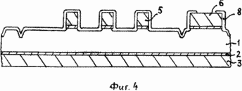 |
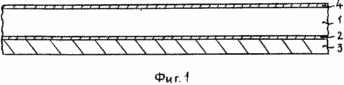
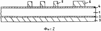
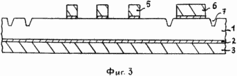
1 - semiconductor plate;
2 - layers of contact metallization of palladium-silver, deposited on the rear of the plate;
3 - galvanically grown layer of silver on the back of the plate;
4 - layers of contact metallization chrome - palladium - silver;
5, 6 - the galvanically grown silver layer of the face-to-face contacts of the photoconverter and the shunting diode;
7 - mesa-grooves along the perimeter of the active region of the photoconverter with a shunting diode;
8 - antireflection coating.
As an example of the implementation of the method, a semiconductor plate with an n-Ge substrate structure, n-GaAs buffer layer, n-GaAs base layer, p-GaAs emitter layer, p + -GaAlAs wide-gap layer, p + -GaAs contact layer is used.
The contact layer of palladium-silver metallization is sprayed onto the rear of the plate. The thickness of the palladium layer is ~ 400 Å, silver ~1000 Å. Alternatively, a gold-germanium alloy of thickness ~ 0.15 μm may be applied. Without removing platinum from the chamber of the sputtering installation, heat treatment is carried out at a temperature of ~ 450 ° C, t = 30 seconds, in vacuum, which is necessary to reduce the resistance of the back contact.
Next, layers of contact metallization of chromium are deposited on the front side of the plate at temperatures of 350 ° C, palladium and silver at a temperature of 250 ° C. Sputtering is carried out directly on the entire surface of the semiconductor.
The thickness of the deposited chromium layers is ~ 300 Å, palladium ~ 400 Å, silver ~1000 Å.
Sputtering a layer of chromium with a thickness of less than 200 Å is impractical due to the through diffusion of palladium. A layer of chromium thicker than 400 Å is undesirable due to an increase in the series resistance of the contacts. A palladium layer is necessary for the adhesive bond of chromium and silver layers. At a palladium layer thickness of less than 200 Å, the bond is not provided due to the interdiffusion of silver and palladium, with a thickness of more than 500 Å, the precious metal consumption is unproductive. When the thickness of the silver layer is less than 500 Å, the adhesion of the subsequent galvanic sediment deteriorates, with thicknesses of the silver layer exceeding 1500 Å, the metal consumption is unproductive.
The adhesion of the chromium contact layer to the surface of the semiconductor increases with increasing plate temperature. The optimum temperature regime is 300 ÷ 350 ° C. At the same time, an annealing of the face-to-face contact metallization required to lower the metal-semiconductor transition resistance is simultaneously performed. At temperatures below 300 ° C adhesion of contact metallization deteriorates. Temperatures above 350 ° C, after deposition of a continuous metallization layer, are undesirable, since thin GaAs epitaxial layers are more sensitive to thermal stresses than the germanium substrate. The resulting surface defects impair the parameters of the photoconverter.
The deposition of layers of palladium and silver is carried out when the plate cools down to 250 ° C, which is useful for reducing thermal stresses in metallization, since the coefficients of thermal expansion of palladium and silver (10.6 · 10 -6 K -1 and 19.2 · 10 -6 K -1 ) is significantly higher than that of chromium and gallium arsenide (respectively, 6.6 · 10 -6 K -1 and 5.82 · 10 -6 K -1 ).
Further, a photoresist protective layer is provided. Use photoresist FP-4-04-T. Increase the back contact by electrochemical deposition of silver. The thickness of the deposited layer is 7 μm. The build-up of the rear contact at the initial stage of manufacturing the photoconverter gives the necessary strength to the fragile plate. Remove the photoresist in dimethylformamide (see FIG. 1).
Create a photoresist mask with a picture of the face-to-face contacts of the photoconverter and the shunt diode. Use photoresist FP-4-04-T. Heat treatment: drying 100 ° C, t = 2 hours. The manifestation in 1% solution of potassium hydroxide (KOH) followed by washing in 0.5% KOH and deionized water. Alternatively, to create a mask, a protective layer of photoresist can be used on the face side of the plate after the galvanic extension of the back contact is performed, which reduces the consumption of the photoresist, but exerts increased requirements for the defect-free and chemical resistance of the protective layer. Further, facial contacts are increased by electrochemical deposition of silver. To do this, the plate is laid back on a rigid carrier, pressed to it by the surface tension forces of the solution. Precipitation does not occur on the rear. The galvanic sediment of thickness 7 μm has a dense small-crystalline structure. The photoresist is removed (see FIG. 2).
Next, the deposited layers of silver and palladium are etched by ion-beam etching using a mask of galvanically thickened contacts. In this case, the chromium layer, whose sputtering speed is much (~ 5 times) less than the total layer of palladium, silver, remains on the plate and protects the surface of the semiconductor from the action of argon ions. The ion source is AI-4-0.15 "Radical", a regime combining accelerated and slow etching,
U = 1000 V, t = 20 min, U = 600 V, t = 5 min, p~8 · 10 -2 mm Hg.
The removal of silver and palladium layers by chemical liquid etching is unacceptable, since an electrochemically deposited layer of silver is first discharged, due to the much higher rate of its etching relative to the thermally sprayed layer.
Remove the chromium layer in an aqueous solution of hydrochloric acid HCl ÷ H 2 O = 1 ÷ 1. Etching is initiated by touching the contacts of the photocouple with an aluminum wire. Effects on silver, palladium and the semiconductor layer of p + -GaAs do not occur.
Create a photoresist mask with a picture of the windows around the perimeter of the active region of the photoconverter and the contact of the shunt diode. Etching gallium arsenide layers to a germanium substrate. In this case, the front contacts of the photoconverter and the shunting diode are electrically isolated. An aqueous solution of orthophosphoric acid and hydrogen peroxide is used: H 3 PO 4 (85%) ÷ H 2 O 2 (30%) ÷ H 2 O = 4 ÷ 1 ÷ 2. Etching time t = 15 min. The photoresist is removed in dimethylformamide (see FIG. 3).
The p + -GaAs layer is blown out of the contact areas of the photoconverter in an aqueous solution of citric acid, citric acid and hydrogen peroxide of the composition: (1M) C 6 H 8 O 7 · H 2 O (1 M) K 3 C 6 H 5 O 7 · H 2 O ÷ H 2 O 2 (30%) = 2 ÷ 2 ÷ 1.
The etching is carried out at a solution temperature of 45 ° C, which ensures removal of the p + -GaAs layer with a thickness of ~0.2 μm in t = 2 min. At room temperature (~ 25 ° C), etching proceeds much slower by a factor of ~ 10, which leads to darkening of silver contacts and degradation of the parameters of the photoconverter. At a higher temperature, above 50 ° C, the selectivity of etching is significantly reduced, which makes it impossible to stop etching on the GaALAs layer in a timely manner.
Further, an antireflection coating is applied, masking the contact areas of the photoconverter and the diode, for welding the external terminals.
Laser cutting and plate separation into chips are performed over the metallized rear, which prevents the chips from splitting and mechanical damage to the separable parts (see FIG. 4).
The proposed method of manufacturing a photoconverter provides a contact with good adhesion and low transient resistance, since the deposition of the contact layer of chromium is carried out at a high temperature on the plate 300-350 ° C. At the same time, the face contacts are annealed.
The thickened Cr / Pd / Ag contacts form self-coincidentally using a single photolithography operation.
The current lead during the electrochemical extension of contacts is carried out on a continuous metal layer, which gives a high uniformity of deposition on large diameter plates.
Ion-beam bleeding of the silver and palladium layers to the chromium layer eliminates the need for applying a protective nickel layer.
Formed contacts have a clear edge geometry.
Galvanic expansion of contacts only where necessary, reduces the consumption of precious metal.
CLAIM
Method for manufacturing a photoconverter on a semiconductor wafer with an n-Ge structure, n-GaAs buffer layer, n-GaAs base layer, p-GaAs emitter layer, p + -GaAlAs wide-gap layer, p + -GaAs contact layer comprising deposition of a contact metallization layer On the rear of the plate, the formation of a protective layer of the photoresist, the build-up of a back contact with the electrochemical deposition of silver, the removal of the photoresist, the deposition of successively layers of contact metallization of chromium 200 ÷ 400 Å thick, palladium 200 ÷ 500 Å thickness, silver thickness 500 ÷ 1500 Å, creating a photoresist mask with a pattern Contacts, electrochemical deposition of silver, removal of the photoresist, bleeding of sprayed layers of contact metallization by ion-beam etching, heat treatment of the plate, creation of a photoresist mask with a picture of the windows along the perimeter of the photoconverter, etching gallium arsenide layers to the germanium substrate, removal of the photoresist, p + GaAs layer outside the contact areas, applying an antireflection coating, characterized in that after the deposition of the contact metallization layer on the rear, the plate is heat-treated, the layers of contact metallization of chromium are successively deposited at a temperature of 300-350 ° C, palladium and silver at a temperature of 200-250 ° C , Etching of sprayed layers of contact metallization by ion-beam etching is carried out before the chromium layer, the chromium layer is removed in an aqueous solution of hydrochloric acid, and bleeding of the p + -GaAs layer outside the contact regions is carried out in an aqueous solution of citric acid, citric acid and hydrogen peroxide at Temperature 40 ÷ 50 ° С.
print version
Publication date 17.02.2007gg
![]()

Comments
When commenting on, remember that the content and tone of your message can hurt the feelings of real people, show respect and tolerance to your interlocutors even if you do not share their opinion, your behavior in the conditions of freedom of expression and anonymity provided by the Internet, changes Not only virtual, but also the real world. All comments are hidden from the index, spam is controlled.