| Start of section
Production, amateur Radio amateurs Aircraft model, rocket-model Useful, entertaining |
Stealth Master
Electronics Physics Technologies Inventions |
Secrets of the cosmos
Secrets of the Earth Secrets of the Ocean Tricks Map of section |
  |
| Use of the site materials is allowed subject to the link (for websites - hyperlinks) | |||
Navigation: => |
Home / Patent catalog / Catalog section / Back / |
|
INVENTION
Patent of the Russian Federation RU2009577
![]()
LOW-TEMPERATURE THERMOELEMENT AND METHOD OF ITS MANUFACTURE
The name of the inventor: Kopaev Vyacheslav Georgievich; Batrak Igor Konstantinovich
The name of the patent holder: Kopaev Vyacheslav Georgievich; Batrak Igor Konstantinovich
Address for correspondence:
Date of commencement of the patent: 1991.06.28
Area of use: direct conversion of thermal energy into electrical energy. SUMMARY OF THE INVENTION: in a low-temperature thermoelement whose branches are made of ternary alloys based on bismuth telluride, the switching layers are made of iron or its alloys and are attached to the end surfaces of the branches, and the middle part of the commutation layer is located on the end surface of the electrical insulating layer. The commutation buses are connected to the switching layers, the ratio of the thickness of the commutation layer and the height of the switching bus is chosen in the range 1: 3 to 10. When manufacturing the thermoelement after pressing the branches of powders of semiconductor materials at room temperature, a switching layer is applied to their end surfaces by means of gas-plasma spraying and Then the commutation bar, followed by hardening by annealing or "hot" pressing. Optimum regimes of gas-plasma sputtering and hardening are given.
DESCRIPTION OF THE INVENTION
The invention relates to the field of direct conversion and can be used in low-temperature thermoelements (i.e., in thermocouples whose hot junction temperature does not exceed 300 ° C during operation), whose branches are made of ternary alloys based on bismuth telluride.
Known is a low-temperature thermoelement containing semiconductor branches of n- and p-type, made of ternary alloys, switching layers based on bismuth antimonide and copper commutation buses [1].
The disadvantage of the known thermoelement is the high cost, which is due to the use of a three-component connection as the material of the switching layer, but also the high cost of the technological switching process, which involves gas-thermal sputtering in a deep vacuum of bismuth antimonide.
The thermoelement containing semiconductor branches of n- and p-types of conductivity made of ternary alloys based on bismuth telluride, connected to them switching layers and commutation buses and an electrical insulating layer located between branches is the closest in technical essence and achieved result to the described low-temperature thermoelement. [2].
In the known thermocouple, high cost is determined, on the one hand, by the considerable cost of the material of the commutation layer, which in the known element is made in the form of compressed plates of nickel antimonide (0.5-0.8 mm thick) with the addition of a plasticizer, since the cost of such a material of the switching layer Comparable to the value of the semiconductor material of the branches; On the other hand, the increased cost of the thermoelement is explained by the high cost of the technological process of commutation with the branches of the switching layers and the switching buses and the subsequent "redundancy".
The method closest to the proposed method is the method of commutating the pressed thermoelements from the Bi 2 Te 3 alloy by gas-plasma spraying of a layer of commutation materials on the surface of thermoelements [3].
The object of the invention is to reduce the cost of a low temperature thermoelement while improving the manufacturing processability thereof.
The specified positive effect is ensured by the fact that it was possible to significantly reduce the cost of the material of the commutation layer, since the cost of iron and its alloys, from which the switching layers are performed in the claimed thermoelement, is more than an order of magnitude less than the material of the switching layer in the known thermoelement, and the thickness Its (0.1-0.25 mm) is several times smaller than the thickness of the commutation layer (0.5-0.8 mm) in the known thermoelement, placing the middle part of the commutation layer on the end surface of the insulating layer contributes to the cost reduction, since the electrical insulation layer serves And this makes it possible to select the thickness of the commutation layer that is minimally necessary to create a reliable barrier (it has been experimentally established that a few years of service life is provided by switching layers 0.1-0.25 mm thick), and a decrease in the thickness of this layer helps to reduce its cost.
In order to obtain minimum losses in commutation buses, it is preferable to make them from materials that have good adhesion to iron and high electrical conductivity, for example aluminum, nickel, etc. Preferably, taking into account the electrical resistance of the material, the height of the commutation tires should be within 0.75-1 mm , Which determines the optimum range of the ratio of the thickness of the switching layer to the height of the switching bus in the range 1: 3-10, since at a lower ratio, the total electrical losses in commutation can sharply increase, and exceeding these ratios by almost an order of magnitude does not lead to a decrease in losses and Causes an increase in cost due to the duration of the gas-plasma spraying process of the material of the switching buses.
Preferably, the switching layers are made of iron or its alloys, for example from low-carbon steels (grade ST 08, CT 10, CT 15, 09KP, etc.), since they have been experimentally set to a high resource stability (resource - several years when operated in an inert Atmosphere at a temperature of hot junctions of 250 ° C), an almost perfect coincidence of the coefficients of thermal expansion of these materials with the KTP of semiconductor ternary alloys from which branches are made, and, in addition, low-alloy steels possess high plasticity, which increases the resource stability in thermal cycling.
The commutation busbars are preferably made of aluminum or its alloys, since along with the high electrical conductivity and cheapness, it is these materials that have excellent adhesion to the iron and its alloys in the gas-plasma spraying thereof.
The use of a layer of less than a branch height and the execution of an arcuate end face allows to minimize the thickness of the switching connections and, consequently, the cost, since a ridge is automatically formed and this allows obtaining a high mechanical strength at the minimum thickness.
The use of the method for manufacturing a thermocouple, which consists of the simultaneous formation of the switching layer and its attachment to the end surfaces of the branches, also contributes to the reduction in cost, immediately after the formation of this layer, the switching buses are connected in 5-20 seconds, gas-plasma spraying allows the switching layer to be formed quickly (less than a minute) It has excellent adhesion to the material of cold-pressed semiconductor branches; The time interval between the application of the switching of the layer and the subsequent application of the material of the switching bus to be less than 5 s is inexpedient, since in a shorter time it is practically impossible to switch to a gas-plasma spraying of another material (tested experimentally), and at an interval of more than 20 s, excessive oxidation of the applied layer is obtained and The same time within 5-20 seconds it is quite possible to switch to the spraying of the material of the switching bus (for example, stopping the feeding of one workpiece and starting the supply of another workpiece).
The connection of the material of the commutation bus to the material of the switching layer makes it possible to significantly simplify the technological process of commutation and, accordingly, to reduce the cost of the thermoelement.
The final operation of the method is the hardening of the multilayer semiconductor system - the switching layers - the switching buses using heat treatment. Preferably, in the gas-plasma spraying of the switching layers, the billet of iron or its alloys is fed into the plasma forming zone (in comparison with the commonly used workpiece in the form of a powder, the use of a wire reduces the cost and, most importantly, the effect of the oxidation of the surface of the powder particles is eliminated). It has been experimentally established that the optimum diameter range of the supplied wire is 0.5-1 mm, since at a smaller diameter fine particles are formed which are poorly sprayed due to partial combustion, and at a diameter exceeding 1 mm, the nozzle is clogged. The wire feed speed is chosen within the range of 1-1.6 mm / s, because at a lower feed rate the continuity of the sputtering process is not ensured and the process is accordingly tightened, and at a speed exceeding 1.6 mm / s, Wires and it is necessary to increase unnecessarily the expended power, which leads to an increase in the cost of manufacture.
The regimes of gas-plasma sputtering of iron on cold-pressed semiconductor branches or its alloys (for example, low-alloy steels) have been experimentally established, since the power consumed by the plasmatron is chosen within the limits of 7.6-12.0 kW at a current of 320-400 A, since at lower values of power And current values), it is not possible to achieve a sufficiently uniform layer - it is difficult to obtain a stable deposited medium, and at a power of more than 12 kW (and a current of more than 400 A), there is no further improvement in the quality of the deposited layer and an increase in electricity consumption, and, accordingly, the cost.
The inert gas consumption (usually argon) is chosen within the limits of 25-40 l / min, since at a lower flow rate the instability of the jet is observed and the process of sputtering is unstable.
The optimal parameters of the regime of gas-plasma deposition of aluminum or its alloys have been experimentally established: the wire feed speed is 1.5-2 mm / s, the wire diameter is 0.8-1 mm, the power is 5-8 kW, and the gas consumption is 18-25 l / min.
The processes of additional hardening of semiconductor-switching layer structures - switching buses, which are obtained after gas-flame spraying, are experimentally optimized, which makes it possible to improve the thermomechanical strength along with the increase in efficiency. Thus, when annealing is strengthened by annealing, the annealing temperature is chosen in the range of 400-450 ° C. As a result, it is at such temperatures that a good additional adherence of particles in all layers of thermoelements and layers is ensured. At lower temperatures and an annealing time of less than 2 h, the hardening is not sufficient, at a temperature above 450 ° C and a time of less than 1 h, sublimation of the semiconductor material sharply increases. When using hot pressing, the pressure is selected in the range 3.5-4.5 t / cm 2 , since at lower pressures reliable adhesion is not ensured, and at pressures exceeding 4.5 t / cm 2 , repressions are observed - excessive creep Branches, the influence of temperatures corresponding to these pressures is similar, and the duration of the "hot" pressing process is chosen in the range of 3-7 minutes, with a shorter duration of the process, complete formation of structures is not observed, with longer time - re-pressing.
 |
 |
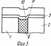 |
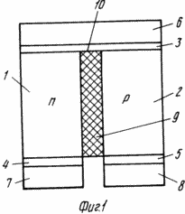
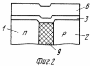
In Fig. 1 shows a low-temperature thermoelement; In Fig. 2 - the same with a rectangular ridge in the commutation bus; In Fig. 3 - the same with an arcuate ridge.
The low-temperature element contains semiconductor branches of n- and p-types 1 and 2, switching layers 3-5, the commutation buses 6-8 connected to them, an electrical insulating layer 9 with an end surface 10, an end 11 of the electrical insulation layer.
Semiconductor branches of n- and p-types are preferably made of ternary alloys based on bismuth telluride (n-type Bi 2 Te 3 -Sn 2 Te 3 , p-type Bi 2 Te 3 -Sb 2 Te 3 with dopant impurities) The switching layers 3-5 are made of iron (with a purity of 99.9-99.7%) or its alloys (preferably from low-carbon steels, for example from steels SG 08, ST 10, ST 15 , 09KP, etc., as having maximum plasticity). The commutation layer 3 is connected by gas-flame spraying to the end faces of the branches 1 and 2 which are oriented perpendicularly to the pressing direction, the middle part of the commutation layer 3 being located on the end surface of the electrical insulating layer 9. The commutation bus 6 is connected by means of gas-plasma spraying to the switching layer 3, 7 and 8, respectively, to the switching layers 4 and 5. The electrical insulation layer 9 can be buried in relation to the end faces of the branches 1 and 2 to a depth not exceeding the thickness of the switching layer 3 (see Figure 3), in which case the end of the switching The interlayers are combined with the corner edges of the branches 1 and 2. The bus bars 6-8 are preferably made of aluminum or its alloys.
EXAMPLE. At room temperature, from the powders of semiconductor materials made from ternary alloys based on bismuth telluride, at a pressure P 1 = 5 tons / cm 2, branches with a cross section of 3x3 mm and a height of 5 mm are pressed. Branches are glued with drops of epoxy resin to a layer of polyimide 0.3 mm thick, placing the end surface of the film flush with the surface of the branches. Then, gas plasma spraying is carried out on the plasma unit UCP-3D using a preform from a wire of the ST 10 grade fed to the plasma formation zone at a speed of 1.2 mm / s, with a power consumption of 9 kW, a current of 350 A and an argon flow of 30 liters per minute. Spray the CT 10 patch layer 0.15 mm thick onto a surface perpendicular to the "cold" pressing plane, three nozzle passes above the surface of the branches. Spraying is carried out through a window that repeats the shape of the switching bus. Then a layer of aluminum alloy AMC 1 mm thick is sprayed under the following conditions: wire feed speed 1.5 mm / s, wire diameter 1 mm, power 5.5 kW, argon consumption 20 l / min. Further, these operations for spraying the switching layers from CT10 and the layers of commutation tires from the AMC are carried out on opposite surfaces of the semiconductor branches. In conclusion, the formed billet is annealed at 440 ° C for 100 minutes in an argon atmosphere. Measurement of the characteristics of the manufactured thermoelement showed that its thermoelectric power in the 200 ° C drop coincides with the thermoelectric power of the base object, and the resistance of the switching connections is less by 1%.
The manufactured low-temperature thermoelement (see Figure 1) works as follows. On the hot junctions of the semiconductor branches 1 and 2, through the commutation bus 6 and the switching layer 3, a heat flux arrives, creating a temperature difference on branches 1 and 2. Due to the Seebeck effect, a thermal EMF is generated, and from the end commutation buses 7 and 8, the generated electrical energy is supplied to the payload. When heated to 250 о С, thermal expansion of the switching bus 6 and the switching layer 3 takes place, the middle part of which rests on the end surface of the electrical insulation layer 9. During prolonged operation (2000 hours or more), the performance of the thermoelement did not deteriorate. (56) 1. The author's certificate of the USSR N 323823, cl. H01L 35/34, 1970.
2. Author's certificate of the USSR N 704397, cl. H 01 L 35/04, 1978.
3. Authorship of the USSR N 199946, cl. H 01 L 35/34, 1965.
CLAIM
1. A low-temperature thermoelement comprising semiconductor branches of n- and p-types of conductivity made of ternary alloys based on bismuth telluride, commutation buses connected to the branches by means of switching layers, and an electrical insulating layer located between the branches, characterized in that, for the purpose Reducing the cost while increasing the manufacturability of the fabric, the switching layers are made of iron or its alloys, the middle part of the switching layer being located on the end surface of the electrical insulation layer, and the ratio of the thickness of the switching layer and the height of the switching bus is 1: 3-10.
2. A thermoelement according to claim 1, characterized in that the switching layers are made of low-alloy steel.
3. An element according to claim 1, characterized in that the commutation busbars are made of aluminum or its alloys.
4. Element according to claim 1, characterized in that the branches are made in the form of rectangular parallelepipeds, the electrical insulation layer is attached to the lateral surfaces of the branches, the height of the electrical insulating layer being less than the height of the branches.
5. The thermoelement according to claim 1, characterized in that the end surface of the electrical insulating layer has an arcuate shape, the commutation layer being adjacent to the electrical insulating layer.
6. A method of manufacturing a low temperature thermoelement by pressing the branches of ternary alloy powders based on bismuth telluride at room temperature, gas-plasma sputtering of the commutation layer and subsequent gas-plasma spraying of the commutation bar, characterized in that the gas-plasma spraying of the commutation layer is carried out simultaneously on the end faces of the cold-pressed branches and the electrical insulating layer , Located between the branches, after 5-20 seconds a gas-plasma spraying of the commutation bar is carried out and then additional hardening is carried out using heat treatment.
7. A method according to claim 6, characterized in that, when gas-plasma spraying the switching layer into the plasma formation zone, the end of the billet is moved in the form of a wire 0.5-1 mm in diameter from iron or its alloys at a speed of 1-1.6 mm / This is the choice of the following mode of plasma formation: power consumption 7.6-12 kW at a current of 320-400 A and an inert gas flow of 25-40 liters per minute.
8. The method of claim 6, characterized in that the additional hardening is carried out by hot pressing in a direction perpendicular to the pressing direction in the manufacture of the branches, under the following conditions: pressure 3.5-4.5 tons / cm 2 , temperature 350-370 ° C, time 3 - 7 min.
9. A method according to claim 1, characterized in that additional hardening is carried out by annealing the branches with the deposited layers in an inert atmosphere at 420-450 ° C for 1.5-2 hours.
print version
Published on February 13, 2007
![]()

Comments
When commenting on, remember that the content and tone of your message can hurt the feelings of real people, show respect and tolerance to your interlocutors even if you do not share their opinion, your behavior in the conditions of freedom of expression and anonymity provided by the Internet, changes Not only virtual, but also the real world. All comments are hidden from the index, spam is controlled.