| Start of section
Production, amateur Radio amateurs Aircraft model, rocket-model Useful, entertaining |
Stealth Master
Electronics Physics Technologies Inventions |
Secrets of the cosmos
Secrets of the Earth Secrets of the Ocean Tricks Map of section |
  |
| Use of the site materials is allowed subject to the link (for websites - hyperlinks) | |||
Navigation: => |
Home / Patent catalog / Catalog section / Back / |
|
INVENTION
Patent of the Russian Federation RU2279748
![]()
DEVICE FOR CHARGING CHARGER CONDENSER
The name of the inventor: Victor Meshcheryakov (RU); Koval Alexey Anatolyevich
The name of the patent holder: LIPETSK STATE TECHNICAL UNIVERSITY (LSTU)
Address for correspondence: 398600, Lipetsk, ul. Moscow, 30, LSTU, NIS
Date of commencement of the patent: 2005.03.09
The invention relates to pulse technology and relates to capacitive storage of electrical energy. It can be used in the implementation of the so-called "slow" charge for several periods of the supply voltage, for charging capacitive storage devices of electric energy (EEEE), generators of powerful pulses. The essence of the invention consists in that current-limiting-dosing elements are made in the form of coils of inductance, the bridge converter is made in the form of an autonomous voltage inverter on lockable keys, three-phase network voltage inputs are additionally connected to the outputs of a three-phase power supply, the outputs of which are connected to one inputs of the control unit , The inputs of the three-phase bridge converter are additionally connected to the inputs of the phase current sensors whose outputs are connected to other inputs of the control unit, a voltage sensor of the capacitive accumulator is connected to the output of the three-phase bridge converter, the output of which is connected to another input of the control unit, Set the value of the voltage of the drive, another output of the control unit is connected to the output of the unit for setting the charge tempo of the drive. As a result, the presented device provides a technical result - a high speed charge of the capacitive accumulator to a voltage exceeding the amplitude of the line voltage of the network by several orders of magnitude. The principles of the control system construction allow to realize in a wide range the smooth regulation of the charge speed of the capacitive storage device, while the current draws almost sinusoidal current from the network, and the use of inductors instead of current-limiting capacitors increases the reliability of the device.
DESCRIPTION OF THE INVENTION
The invention relates to pulse technology and relates to capacitive storage of electrical energy. It can be used in the implementation of the so-called "slow" charge for several periods of the supply voltage, for charging capacitive storage devices of electric energy (EEEE), generators of powerful pulses.
A device is known for charging a capacitive energy storage device comprising a three-phase alternating current source with three leads, a capacitive energy storage device, a first metering capacitor, a second metering capacitor whose one cover is connected to the first terminal of a three-phase alternating current source, a charging thyristor whose cathode is connected to the first terminal A cathode of the second is connected to the third terminal of a three-phase alternating current source, the anode of the third is connected to the second terminal of a three-phase alternating current source and the control unit of the system, the first, second and third terminals of which Are connected with the first, second and third terminals of the three-phase alternating current source respectively, and the fourth and fifth terminals thereof, with the control switching of the charging thyristor, additionally provided with a linear choke with two terminals and a tapping from a part of its windings, the first terminal of which is connected to another plate of the second metering Capacitor, a second terminal to the second terminal of the capacitive accumulator, and a tap to the anode of the second valve, thyristors are used as the first, third and fourth valves, the charging thyristor anode is connected to the other plate of the first metering capacitor and to the cathode of the third thyristor, The thyristor is connected to the second terminal of the linear throttle, the anode of the fourth thyristor is connected to the third terminal of the three-phase alternating current source, and its cathode with the anode of the first thyristor, the sixth and seventh terminals of the system control unit are connected to the control transition of the first thyristor, The ninth of its conclusions to the control transition of the third thyristor, the tenth and eleventh leads to the control transition of the fourth thyristor, the twelfth and thirteenth leads to the first and second terminals of the capacitive accumulator, and the fourteenth and fifteenth terminals to one and the other plates of the second metering capacitor [1 ].
Disadvantages of this device are as follows: first, it provides the charge of the capacitive storage device to a relatively low voltage (low specific energy indicators); Secondly, the low rate of energy storage, and the absence of smooth control over a wide range of speed (the rate of voltage growth on the plates of the storage capacitor) charge; Thirdly, the consumption of current from the network with a high non-sinusoidal coefficient; Fourth, the circuit solution of the device does not allow creating a flexible high-speed control system.
The closest in technical essence to the present invention is a device for charging a capacitive energy storage device comprising a three-phase alternating current source with three output terminals, a three-phase full-wave bridge thyristor rectifier with two output terminals for connecting a storage capacitor and three input terminals, each of which through current- The metering capacitor is connected to the output terminals of the alternating current source and the voltage control and phase control unit of the rectifier thyristors, an additional thyristor is provided, and the voltage control and phase control unit of the thyristors is provided with an additional output that is connected to the control electrode, the thyristor cathode and one of the input terminals of said rectifier , While the positive output terminal of the rectifier is connected to the anode of this thyristor [2].
Disadvantages of this device are: firstly, the limited use due to the fact that it provides charge of the capacitive accumulator to a voltage that is 3 times greater than the amplitude of the line voltage of the source, which indicates low specific energy parameters (ie, the ratio of power, Mass of the charge device); Secondly, the absence of a smooth and wide range of regulation of the rate of charge of the capacitive storage; Third, the unsatisfactory form of the current consumed from the supply network; Fourthly, the presence of less capricious in use current-limiting-dosing capacitors.
The technical result of the invention consists in that, a device for charging a storage capacitor comprising a three-phase power supply whose outputs are connected to one terminals of three current-limiting-metering elements whose other terminals are connected to the inputs of a three-phase bridge converter whose outputs are connected to a storage capacitor, The outputs are connected to the control inputs of a three-phase bridge converter, characterized in that the current limiting-dosing elements are made in the form of coils of inductance, the bridge converter is made as a self-contained voltage inverter on lockable keys, the inputs of a three-phase network sensor The outputs of which are connected to one inputs of the control unit, the inputs of the three-phase bridge converter are additionally connected to the inputs of phase current sensors whose outputs are connected to other inputs of the control unit, a voltage sensor of the capacitive accumulator is connected to the output of the three-phase bridge converter, the output of which is connected to another input of the block The input of the unit for setting the value of the drive voltage is connected to the other input of the control unit, and the output of the unit for setting the charge tempo of the drive is connected to one input of the control unit.
 |
 |
||
 |
 |
||
| |||
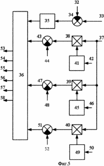
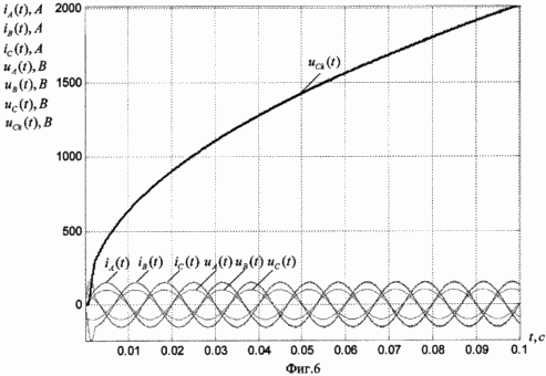
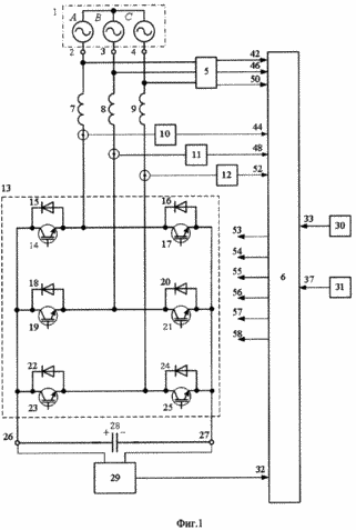
FIG. 1 is a block diagram of an apparatus for charging a storage capacitor; FIG. FIG. 2 shows a principal power circuit of the device in the first operation cycle; FIG. 3 is a schematic diagram of the replacement of the proposed device, explaining its operation in the first step; 4 is a schematic diagram of a device replacement, explaining its operation in the second clock cycle; FIG. 5 is a block diagram of the control unit; FIG. 6 shows graphs obtained as a result of modeling the operation of the device. FIG.
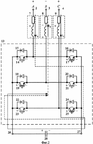
The block diagram of the device for charging the storage capacitor of FIG. 1 comprises: a three-phase AC source 1 with three output terminals 2, 3 and 4 to which the inputs of the three-phase voltage sensor of the network 5 are connected, the outputs of which are connected to the inputs of the control unit 6, Output terminals of the alternating current source and are connected to one of the terminals of the respective phase inductors 7 (phase A), 8 (phase B), 9 (phase C), other inductor terminals 7, 8 and 9 are connected to one terminals of the current sensors 10, 11 and 12 (Current feedback realization) whose outputs are connected to other inputs of the BU 6, other terminals of the current sensors 10, 11, and 12 are connected to the input of an autonomous three-phase voltage inverter (AIN) 13 made on fully controllable switches (IGBT transistors) 14, 17, 19, 21, 23 and 25 with the return diodes 15, 16, 18, 20, 22 and 24, a capacitive accumulator 28 is connected to the output terminals of the inverter 26 and 27, the plates of which are connected to the inputs of the voltage sensor of the accumulator 29 from whose output the signal Corresponding to the drive voltage is supplied to the VU 6, the VU 6 receives the signals of the drive voltage value from the unit 30 and the charge rate of the accumulator from the unit 31.
Consideration of the work of the device should be carried out by analyzing two strokes of the work
The first step is the principal power circuit of the device (see Fig. 2) and the substitution circuit (see Fig. 3). To simplify the description, we assume that the capacitor 28 is already charged through the reverse diodes of the keys (the charge current circuit, and therefore the diodes participating in the charge transient process, are determined by the instantaneous values of the phase voltages of the network, at the moment of connection of the AIN 13 to the AC network). The result of the transient process will be the presence on the plates of the capacitor 28 voltage, the potential of which is higher than the amplitude values of the line voltage of the network and the current flow through the reverse diodes is impossible. From this moment, the process of charging the storage capacitance is controlled by the VU 6.
The BU 6 controls the device with priority requirements:
- consumption from the network of currents with a shape as close as possible to the sinusoidal;
- power factor of the device, close to unity;
- the possibility of ensuring the maximum possible speed of the process of energy storage in the drive.
Let us analyze the process of accumulation of energy, for the beginning take the moment of time t 1 , corresponding to the moment of changing the sign of the voltage of phase A from the negative half-wave to positive.
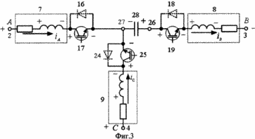
Referring to FIG. 3, a first operation cycle of the device will be described.
BU 6 generates control pulses for the opening of transistors 17, 19 and 25. As a result, chains are formed for the flow of a system of three-phase currents i 2 (t), i 3 (t), i 4 (t).
In FIG. 3, the circuit for the current i 2 is 2-7-17-27-28-26-19-8-3, i.e. The voltage of the capacitor 28 turns on according to the linear voltage u 23 (t) (here and below the element through which the current does not flow is shown as a dashed line) and, as a consequence, the current transient i 2 (t) is characterized by its growth. This process can be described by the equations:
![]()
![]()
Where C is the capacity of the storage capacitor 28;
I A (t) = i 2 (t) is the instantaneous value of the phase current A;
R A - resistance of the inductor 7 phase A;
L A - inductance of inductor 7 of phase A;
L B - inductance of the inductor 8 phase B;
R B - resistance of the inductor 8 phase B;
U AB (t) = u 23 (t) is the line voltage between phases AB.
3 shows the current flow circuit i 4 (t) 4-9-25-27-28-26-19-8-3, i.e. The voltage of the capacitor 28 turns on according to the linear voltage U BC , as a consequence, the current transient i 4 (t) is characterized by its growth. This process can be described by the equations:
![]()
![]()
Where i C (t) = i A (t) is the instantaneous current value of phase C;
L C - inductance of the inductor 9 phase C;
R C - resistance of the inductor 9 phase C;
U BC (t) = u 34 (t) is the line voltage across the phases of the aircraft.
In Figure 3, the circuit for the current i 3 (t) is two parallel branches of the currents i 2 (t) and i 4 (t), so the instantaneous value of the current i 3 (t) is equal to the sum of these currents:
![]()
Derivatives of the actual phase currents are high enough, as a result they exceed the given current, BU 6 will work to reduce the phase current, namely disconnect switches 17, 19 and 25. This moment is designated as t 2 .
From this moment the growth of the phase currents stops, and the energy of the magnetic field accumulated in the magnetic field of the inductors 7, 8 and 9 starts to support the current in the same direction. The direction of the currents for the phases will be preserved, but the chain of their flow to the AIN will change. In this case, the reverse diodes of the keys are the circuits for transferring the energy of the magnetic field of the inductors.
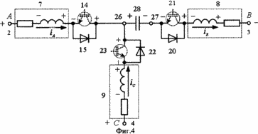
Consider the second step of the device operation (see FIG. 4).
FIG. 4 shows a circuit for flowing current i 2 (t) 2-7-15-26-28-27-20-8-3, i.e. The voltage of the capacitor 28 turns on opposite to the linear voltage u 23 (t), as a consequence, the current transient i 2 (t) is characterized by its decrease. This process can be described by the equations:
![]()
![]()
In FIG. 4, the chain for the current i 4 (t) is 4-9-22-26-28-27-20-8-3, i.e. The voltage of the capacitor 28 turns on opposite to the linear voltage U BC , as a consequence, the transient process but to the current i 4 (t) is characterized by its decrease. This process can be described by the equations:
![]()
![]()
In FIG. 4, two parallel branches of currents i 2 (t) and i 4 (t) are the circuit for the current i 3 (t), therefore the instantaneous value of the current i 3 (t) is equal to the sum of these currents according to the expression (5).
The process of charging the storage tank 28 is accompanied by a decrease in currents below the set values, the VU 6 operates to increase the phase currents, thus giving signals for the opening of the keys 17, 19, and 25, then the processes are repeated.
Energetically, the process of accumulation of electrical energy in a capacitive storage device is the following successive processes: the first cycle is the accumulation of energy in the magnetic field of inductors 7, 8 and 9, the second cycle is the return of this energy to the storage ring 28, i.e. Conversion of the energy of the magnetic field of the inductors 7, 8 and 9 into the energy of the electric field of the capacitor 28. During these two cycles in the condenser, the stored energy will increase by the amount:
![]()
Where ![]() U C - voltage increment on the capacitor plates 28.
U C - voltage increment on the capacitor plates 28.
In the next cycle of energy storage in the magnetic field of the inductors 7, 8 and 9, the previous increment ![]() U C to the voltage of the capacitor 28 will lead to an increase in the derivative currents
U C to the voltage of the capacitor 28 will lead to an increase in the derivative currents ![]() , That in the subsequent recoil cycle will lead to an increase in the output energy of the magnetic field of the inductors 7,8 and 9. The following increment
, That in the subsequent recoil cycle will lead to an increase in the output energy of the magnetic field of the inductors 7,8 and 9. The following increment ![]() U C influences the process in a similar way and so on.
U C influences the process in a similar way and so on.
Thus, the accumulation is characterized by the process of "swinging" the system of inductors 7, 8 and 9 of the accumulator 28, in which each previous accumulation cycle feeds the subsequent one. This allows us to conclude that a half-period increase in the amplitudes of the phase currents is possible:
![]()
![]()
![]()
Where ![]() I m is the increment of the amplitudes of the phase currents.
I m is the increment of the amplitudes of the phase currents.
In this device, the principle of accumulation with constant amplitudes of phase currents is applied, while the functional dependence of the capacitance voltage on the time u C (t) is close to the hyperbola. The specified amplitude of the phase currents determines the growth rate u C (t). In this case, the maximum possible storage capacitor voltage, as well as the maximum accumulation rate, are determined by the permissible characteristics of the device circuit elements, such as the maximum permissible transistor current, the switching frequency, the maximum allowable voltage on the capacitance, and so on.
Consider the work of BU 6 (see Fig. 5). The VU 6 monitors the current value of the voltage on the plates of the storage tank 28 by comparing the signal proportional to this voltage u Ck (t) entering the input 32, with a given value U *C entering the input 33, in the comparison unit 34, the difference (U *C -u Ck (t)). The output of the unit 34 is connected to the input of the relay unit 35 in which a logic signal is generated for blocking the supply of the control pulses of the AIN keys and for disabling the accumulation mode based on comparing the input quantity with the setpoint. The output of block 35 is entered into the AIF 36. The charge rate is determined by the magnitude of the amplitude of the phase currents, a signal proportional to the amplitude comes from block 31 to input 37 of BU 6. The formation of the specified phase currents is performed in three parallel branches. Consider the control channel for the current in phase A. The task for each chain is to set the amplitude of the currents I m 37, which is fed to the inputs of the multiplying blocks 38, 39 and 40. The second input of the block 38 is the signal from the output of the conversion unit 41, Proportional to the voltage of phase A. The coefficient of block 41 is the ratio
![]()
Where U m.oc. Is the amplitude of the feedback signal of the phase voltage.
As a result, at the output of block 41 a signal will be received:
![]()
Thus. At the output of block 38:
![]()
The output of the unit 38 comes to the input of the comparison unit 43, in which the value of the set current is compared with the current feedback 44 i 2ist (t).
The output of block 43 goes to the AIF 36.
Similarly, the current channels i 3* (t), i 4* (t).
When BU 6 is built on the basis of microprocessor technology, high speed, accuracy, versatility and adaptability of the device are achieved, which significantly expands the scope of its use.
FIG. 6 shows the results of modeling a three-phase controlled capacitive accumulator using the MatLab R12 6.0 program in the Simulink 4.0 package with the Power System Blockset extension.
In FIG. 6, during the simulation of 0.1 s, the voltage across the capacitor plates of 1000 uF capacitance exceeded the amplitude of the phase voltages by more than 20 times, while a sinusoidal current was consumed from the network (the time of uncontrolled spontaneous charge of the capacitance as a result of the transient is insignificant; Is about 25% of the half-period of the supply voltage).
Thus, the replacement of current limiting dosing capacitors with inductors of the make-up and the use instead of thyristors in a three-phase full-wave rectifier bridge rectifier of the lockable keys and the reverse diodes connected in parallel with them led to a change in the principle of energy storage in the drive, unlike the prototype. As a result, the presented device provides a high rate of charge of the capacitive accumulator to a voltage exceeding the amplitude of the line voltage of the network by several orders of magnitude, which indicates high specific energy indices. The principles of BU 6 construction allow to realize in a wide range a smooth regulation of the charge speed of a capacitive storage device, while the current draws almost sinusoidal current from the network, and the use of inductors instead of current-limiting capacitors increases the reliability of the device.
INFORMATION SOURCES
1. Device for charging the storage capacitor. Dodotchenko VV, Nikolaev AG, Bystrov VK; RU No. 2071167 C1, 6 H 03 K 3/53 1996.
2. A method of charging a capacitive storage of electrical energy and a device for its implementation (variants). Nikolaev AG, Bystrov VK; RU № 2218654 С2, Н 02 М 7/162, 2003.
CLAIM
A device for charging a storage capacitor comprising a three-phase power supply whose outputs are connected to one of the terminals of three current-limiting-metering elements whose other terminals are connected to the inputs of a three-phase bridge converter whose outputs are connected to a storage capacitor, a control unit whose outputs are connected to the control inputs of a three-phase Bridge converter, characterized in that the current-limiting-dosing elements are made in the form of coils of inductance, the bridge converter is made in the form of an autonomous voltage inverter on the lockable keys, the inputs of a three-phase mains voltage sensor are additionally connected to the outputs of the three-phase power supply, the outputs of which are connected to one inputs of the control unit , The inputs of the three-phase bridge converter are additionally connected to the inputs of the phase current sensors whose outputs are connected to other inputs of the control unit, a voltage sensor of the capacitive accumulator is connected to the output of the three-phase bridge converter, the output of which is connected to the other input of the control unit, Set the value of the voltage of the drive, another output of the control unit is connected to the output of the unit for setting the charge tempo of the drive.
print version
Publication date 07.02.2007gg
![]()

Comments
When commenting on, remember that the content and tone of your message can hurt the feelings of real people, show respect and tolerance to your interlocutors even if you do not share their opinion, your behavior in the conditions of freedom of expression and anonymity provided by the Internet, changes Not only virtual, but also the real world. All comments are hidden from the index, spam is controlled.