| Start of section
Production, amateur Radio amateurs Aircraft model, rocket-model Useful, entertaining |
Stealth Master
Electronics Physics Technologies Inventions |
Secrets of the cosmos
Secrets of the Earth Secrets of the Ocean Tricks Map of section |
  |
| Use of the site materials is allowed subject to the link (for websites - hyperlinks) | |||
Navigation: => |
Home / Patent catalog / Catalog section / Back / |
|
INVENTION
Patent of the Russian Federation RU2292627
![]()
SOURCE OF SECONDARY POWER SUPPLY
Compensation of distortions in the feeding network
The name of the inventor: Tereshkov Vladimir Vasilyevich (RU); Korchagin Alexander Vladimirovich (RU); Avanesov Vladimir Mikhailovich
The name of the patent holder: State Educational Establishment of Higher Professional Education "Taganrog State Radio Engineering University" (TRSTU)
Address for correspondence: 347928, Rostov Region, Taganrog, GSP-17A, Nekrasovsky, 44, TSURE
Date of commencement of the patent: 2005.06.30
The invention relates to electrical engineering and can be used in the construction of secondary power sources operating in alternating voltage supply networks with load powers commensurate with the power of the power transformer or autonomous power systems of limited power. The purpose of the invention is to expand the functionality of the device: compensation of inactive (reactive power and distortion power) of the total power component in a single-phase alternating-current network of limited power, improving the quality of the supply voltage, reducing power loss and voltage in the mains. The goal is achieved in that an adaptive regulator is introduced into the secondary power supply with distortion compensation in the power supply network, which modifies the input signal for the control system in such a way that harmonic components of the consumed current injected into the supply network minimize the distortion of the shape of the supply voltage curve at the connection point Claimed device.
DESCRIPTION OF THE INVENTION
The proposed invention relates to electrical engineering and can be used in the construction of secondary power sources operating in alternating voltage power supply networks with load powers commensurate with the power of the power transformer or stand-alone power systems of limited power.
The device "Stabilized voltage source with low-frequency power factor correction" is known [RF patent 2187879, МПК7 Н 02 М 7/12, published on 20.08.2002].
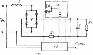 |
The device comprises (Fig. 1) a source of sinusoidal voltage; A series-connected rectifier V and a reactor L connected between a sinusoidal voltage source and an output capacitive filter C with a load R n ; A key circuit SC, connected in parallel to the rectifier input, which provides energy storage in the throttle inductance and isolation from the capacitive filter during the open key state; A control circuit for the SS key connected to the input and output of the stabilized voltage source and the timing control and the duration of the open state of the key in the first half of each half-cycle of the supply voltage; Connected to the key management circuit, the source of a stable constant reference voltage U of the supports and the current sensor Dt, connected between the output of the rectifier and the load, one of the power terminals of the key being integrated with the current sensor terminal connected to the load terminal. The technical result is to give the source function of stabilizing the output voltage. |
Disadvantages of such a device: the possibility of applying for power factor correction only at low frequencies and only at fixed loads.
The reason preventing the achievement of the technical result is the lack of control taking into account the signal about the voltage in the load.
The characteristics of the analogue coincide with the essential features of the claimed invention: the device comprises a single-phase bridge diode rectifier, a control system, a choke; In parallel with the load, a smoothing capacitor is switched on, and in series with the load, a current sensor.
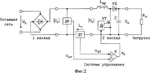
The device "Electronic control gear" is known [Berezin M.Yu., Kovalev Yu.I., Remnev A.M. Methods for improving the power factor of the ballast. - Lighting engineering, 1997, №2, С.6 ... 8]. The device comprises (FIG. 2) a two-stage single-phase power factor corrector and a control system. The first stage forms a single-phase bridge rectifier, the second stage is a dc-type up-converter of the DC voltage, whose output is connected to the load. In the composition of a DC-type impulse converter of a boost type, there are series-connected chokes L dr and a cut-off diode VD, a power transistor VT is connected to the junction of the throttle and the diode. In parallel to the load, a smoothing capacitor C is included. The control system includes a voltage input sensor DV, a current sensor DT, a comparator K. The control system and the second stage of the power factor corrector (the gate circuit of the power transistor VT) are coordinated using the driver device Dr, Second cascade. Generation of the in-phase current curve i n is carried out by comparing the signal u dt from the current sensors DT and the signal u dn from the voltage sensor DV and forming the signal s to the switching by the power transistor VT at the output of the comparator K.
Disadvantages of such a device: the possibility of using only for fixed loads and in devices where high requirements to stabilize the output voltage UH are not required.
The reason preventing the achievement of the technical result is the lack of feedback (control taking into account the signal about the voltage in the load).
The characteristics of the analogue coincide with the essential features of the claimed invention: the device comprises a two-stage single-phase power factor corrector and a control system; The first stage forms a single-phase bridge diode rectifier, the second stage is a switching DC-voltage converter of an up-type type, the output of which is connected to the load; In the composition of the DC voltage impulse converter of the up-type type are series-connected choke L dr and a cut-off diode VD, a power transistor VT is connected to the junction of the throttle and the diode; Smoothing capacitor C is connected in parallel with the load; The control system includes an input voltage sensor DV, a current sensor DT, a comparator K; The coordination of the control system and the second stage of the power factor corrector (gate circuit of the power transistor VT) is carried out using the driver device Dr, which is part of the second stage.
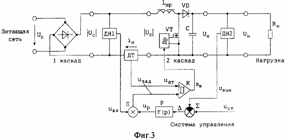
A device is known - a prototype "Scheme of a step-up DC-to-DC converter, used to correct the power factor" [Florentsev SN. Active correction of the power factor of converters with single-phase rectifier at the input. - Electrical Engineering, 1992, N3, p.28 ... 32]. The device comprises (FIG. 3) a two-stage single-phase power factor corrector and a control system. The first stage forms a single-phase bridge diode rectifier, the second stage is a DC-type DC voltage pulse converter whose output is connected to the load. In the composition of a DC-type impulse converter of a boost type, there are series-connected chokes L dr and a cut-off diode VD, a power transistor VT is connected to the junction of the throttle and the diode. In parallel to the load, a smoothing capacitor C is included. The control system includes voltage sensors DN1, DN2, current sensor DT, comparator K, multiplier P, regulator P with transfer function F (p), adder ![]() . The coordination of the control system and the second stage of the power factor corrector (control circuit of the power transistor VT) is carried out using the driver device Ap, which is part of the second stage. Generation of the in-phase current curve i n is carried out by comparing the signals from the current sensors DT and dt and the reference signal u behind the output of the multiplier II and forming the signal s to the switching by the power transistor VT at the output of the comparator K. The reference signal u back is formed by multiplying the signal from the output of the voltage sensor DV1 u in (input voltage of the supply network) and the output signal of the controller u p. The output voltage of the regulator is formed taking into account the discrepancy signal
. The coordination of the control system and the second stage of the power factor corrector (control circuit of the power transistor VT) is carried out using the driver device Ap, which is part of the second stage. Generation of the in-phase current curve i n is carried out by comparing the signals from the current sensors DT and dt and the reference signal u behind the output of the multiplier II and forming the signal s to the switching by the power transistor VT at the output of the comparator K. The reference signal u back is formed by multiplying the signal from the output of the voltage sensor DV1 u in (input voltage of the supply network) and the output signal of the controller u p. The output voltage of the regulator is formed taking into account the discrepancy signal ![]() Between the output signal of the voltage sensor DN2 and out (voltage on the load) and the specified stabilizing signal u st . Disagreement signal
Between the output signal of the voltage sensor DN2 and out (voltage on the load) and the specified stabilizing signal u st . Disagreement signal ![]() Is formed at the output of the adder
Is formed at the output of the adder ![]() .
.
To the lack of the device should be attributed limited functionality: the device does not compensate for the reactive component of full power and power distortion.
The reason preventing the achievement of the technical result is the formation of a common-mode input current. The form of the input current repeats the form of the supply voltage of the network U s and the device does not compensate for the reactive component of the total power and the power of distortions that occur when parallel loads are switched on in parallel (key secondary power supplies with rectifiers at the input and capacitive storage). Thus, the converter is "transparent" to the power supply network only when feeding its own load and does not affect the power quality at the connection point, which can degrade when adjacent non-linear consumers and consumers with a non-unitary power factor (having a reactive component) operate.
The features of the prototype coincide with the essential features of the claimed invention: the device comprises an input voltage sensor, a bridge single-phase diode rectifier, a current sensor, an output voltage sensor, a load, a control system comprising a comparator, a multiplier, a regulator and an adder, In its composition a choke, a cut-off diode, a power transistor, a smoothing capacitor and a driver device, the input of a bridge single-phase diode rectifier being the input of a secondary power supply source with distortion compensation in the supply network, and an input voltage sensor is connected to this input, the upper output of a bridge single-phase diode rectifier is connected With the upper input of the DC voltage impulse converter, and the lower one - through the current sensor - is connected to the lower input of the DC voltage pulse converter, and to the outputs of the latter is connected the output voltage sensor and the load, the outputs of the current sensor and the output voltage sensor are connected respectively to the second and The third inputs of the control system; The first input of the control system is connected to the first input of the multiplier, the output of which is connected to the non-inverting input of the comparator, the second input of the control system is connected to the inverting input of the comparator, the output of the comparator is the output of the control system and carries out switching of the impulse converter of the constant voltage of the boost type, the third and fourth inputs of the control system Are connected respectively to the subtracting and summing inputs of the adder, the output of the latter through the series-connected controller is connected to the second input of the multiplier; The control signal is supplied to the fourth input of the control system.
The objective of the claimed invention is to expand the functionality of the device: compensation of inactive (reactive power and distortion power) of the total power component in a single-phase alternating current network of limited power, improving the quality of the supply voltage and reducing power and voltage losses in the supply network.
The technical result is achieved by the introduction of an adaptive controller in the device for active correction of the power factor of converters with a single-phase rectifier at the input. The adaptive controller modifies the input signal form for the control system so that the harmonic components of the consumed current injected into the supply network minimize distortions in the shape of the supply voltage curve at the point of connection of the secondary power supply source with distortion compensation in the supply network.
In order to achieve a technical result, a device comprising an input voltage sensor, a bridge single-phase diode rectifier, a current sensor, an output voltage sensor, a load, a control system comprising a comparator, a multiplier, a regulator and an adder, a DC type up-converter voltage pulse transducer having a throttle , A cut-off diode, a power transistor, a smoothing capacitor and a driver device, the input of the bridge single-phase diode rectifier being the input of a secondary power supply source with distortion compensation in the supply network, and an input voltage sensor is connected to this input, the upper output of the bridge single-phase diode rectifier is connected to the upper input of the pulse Converter of a constant voltage of a boosting type, and the lower one is connected through the current sensor to the lower input of a pulse converter of a DC voltage of a boost type, and to the outputs of the latter, an output voltage sensor and load are connected, the outputs of the current sensor and the output voltage sensor are connected respectively to the second and third inputs of the control system , And the first input of the control system is connected to the first input of the multiplier, the output of which is connected to the non-inverting input of the comparator, the second input of the control system is connected to the inverting input of the comparator, the output of the comparator is the output of the control system and carries out the commutation of the pulse converter of the DC voltage of the boosting type, the third and fourth inputs The control systems are connected respectively with the subtracting and summing inputs of the adder, the output of the latter through the series-connected controller is connected to the second input of the multiplier, and the fourth input of the control system is supplied with a reference signal, an adaptive controller is added, which includes an adaptive filter, a full-wave rectifier, a calculator, The first input of the adaptive controller is connected to the point combining the input of the adaptive filter, the first input of the calculator and the input of the meter of the power line voltage form factor, and the output of the adaptive filter through the series-connected full-wave rectifier is connected to the first input of the control system, The subtracting input of the summing unit is connected to the output of the meter of the power line voltage form factor, and the signal input of the network voltage form factor is supplied to the summing input, the output of the summation unit being connected to the second input of the calculator whose output line is connected to the input line of the adaptive filter.
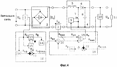
FIG. 4 is a functional diagram of a secondary power source with distortion compensation in the supply network.
The secondary power supply source with distortion compensation in the power supply network includes an input voltage sensor 1, a bridge single-phase diode rectifier 2, a current sensor 3, a dc switching impulse 4 of the upstream type (including a choke 5, a tripping diode 6, a power transistor 7, A smoothing capacitor 8 and a driver device 9), an output voltage sensor 10, a load 11, an adaptive controller 12 (consisting of an adaptive filter 13, a full-wave rectifier 14, a calculator 15, a voltage-form-factor meter 16 and a summation unit 17) and a control system 18 (It consists of a comparator 19, a multiplier 20, a regulator 21 and an adder 22).
The input of a bridge single-phase diode rectifier 2 is the input of a secondary power source with distortion compensation in the supply network. To the input of the source of secondary power supply with distortion compensation in the power supply network, an input voltage sensor 1 is connected whose output is connected to the first input of the adaptive controller 12. The upper output of the bridge single-phase diode rectifier 2 is connected to the upper input of the impulse converter 4 of the constant voltage of the boost type, The current sensor 3 is connected to the lower input of the up-converter DC voltage pulse converter 4. The upper input of the up-converter DC voltage transducer 4 through the throttle 5 is connected to the point to which the anode of the cut-off diode 6 and the drain of the power transistor 7 are connected. The cathode of the cut-off diode 6 is connected to a point connecting the upper plate of the capacitor 8 and the upper output of the DC voltage pulse converter 4 Raising type. The lower input of the up-converter DC voltage transducer 4 combines the source of the power transistor 7, the lower plate of the capacitor 8, and the lower output of the up-converter DC voltage pulse converter 4. The output voltage sensor 10 and the load 11 are connected to the outputs of the latter. The gate and source of the power transistor 7 are connected to the output of the driver device 9 whose input is connected to the output of the control system 18. The outputs of the current sensor 3 and the output voltage sensor 10 are respectively connected to the second and third inputs of the control system 18.
The first input of the control system 18 is connected to the first input of the multiplier 20, the output of which is connected to the non-inverting input of the comparator 19, the second input of the control system 18 is connected to the inverting input of the comparator 19, the output of the latter is the output of the control system 18 and is connected to the input of the driver device 9. The third and The fourth inputs of the control system 18 are connected respectively to the subtracting and summing inputs of the adder 22, the output of the latter through the series-connected controller 21 is connected to the second input of the multiplier 20. The fourth input of the control system 18 is supplied with the reference signal s back .
The first input of the adaptive controller 12 is connected to a point combining the input of the adaptive filter 13, the first input of the calculator 15, and the input of the meter 16 of the power line voltage form factor. The output of the adaptive filter 13 through the series-connected full-wave rectifier 14 is connected to the first input of the control system 18. The subtracting input of the summing unit 17 is connected to the output of the meter 16 of the power factor of the supply network, and the summation input is supplied with a signal for specifying the network voltage form factor s kphase . The output of the summing unit 17 is connected to the second input of the calculator 15, the output line of which is connected to the input line of the adaptive filter 13.
The source of secondary power supply with distortion compensation in the supply network works as follows.
SOURCE OF SECONDARY POWER SUPPLY WITH COMPENSATION OF DISTURBANCES IN THE POWER SUPPLY NETWORK
WORKS AS FOLLOWING
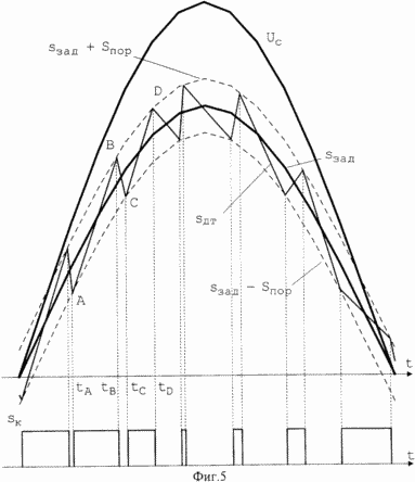 |
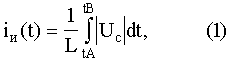
The input alternating single-phase voltage U c is supplied to the input of the input voltage sensor 1 and the input of the bridge single-phase diode rectifier 2. At the output of the input voltage sensor 1, an S c signal ( hereinafter the time function is not shown) is input to the first input of the adaptive controller 12. The output Rectified voltage | U c | (Input signal module) of the rectifier through the current sensor 3 is applied to the input of a DC-type up-converter 4 of a boost type. When the power transistor 7 is switched to the conducting (open) state, the rectified voltage is applied to the throttle 5 | U c | And the current through the throttle i and begins to increase (time interval t A ... t B , Fig. 5):
Where i and (t) is the current source of the stabilized voltage with compensation of distortion power in a single-phase alternating current network; L - inductance of the throttle 5; T A and t B are respectively the times of opening and closing of the power transistor 7. |
In the time interval t A ... t B, the cut-off diode 6 is in the closed state (| U c | <U H ) and the load supply 11 is provided by a charged smoothing capacitor 8. At the output of the current sensor 3, a signal s dt 5 proportional to the input current i And :
![]()
Where k dt is the transmission coefficient of the current sensor 3.
If the output signal of the current sensor 3 exceeds the reference signal s from the output of the multiplier 20 by the value of the threshold signal (hysteresis) of the comparator 19 S, i.e., At s dt -s rear > S pores (point A in Fig. 5), the comparator 19 is switched and the power transistor 7 goes into a closed state. The throttle current is 5 i and flows through the open cut-off diode 6, thereby recharging the capacitance of the smoothing capacitor 8. The current drop in the time interval t B ... t C (FIG. 5) continues to the point C at which s dt -s < S time . At this time, the comparator 19 switches to a single state and the power transistor 7 opens. The current through the throttle 5 increases to the point D, in which s dm -s back > S pores . At the time intervals t A ... t B and t C ... t D, the cut-off diode 6 is closed, i.e. The condition | U c | <U n holds. Thus, a current is formed through the throttle 5 with the envelope in the form of positive half-waves proportional to and repeating the shape of the half-wave voltage U c at the input of the bridge single-phase diode rectifier 2, and therefore at the input of the secondary power supply source with distortion compensation in the supply network.
The output signal s dt of the current sensor 3 is supplied to the inverting input of the comparator 19, where a comparison is made with the reference signal s rear (output of the multiplier 20). Let us express the signal of the multiplier 20 s backwards through a signal of a control error ![]() = S nsd -Un k dn2 at the output of the adder 22 (k dn2 - transmission factor of the sensor 10 output voltage):
= S nsd -Un k dn2 at the output of the adder 22 (k dn2 - transmission factor of the sensor 10 output voltage):
![]()
Where s in is the input voltage of the control system 18;
S out - output voltage signal of the sensor 10 of the output voltage of the device, s out = U n k k dn2 ;
S p - output voltage of the regulator 21;
![]() - voltage at the output of the adder 22;
- voltage at the output of the adder 22;
F (p) is the transfer function of the regulator 21.
The control system 18 provides for the generation of an input current i and whose amplitude is determined by the value of the reference signal s back (output voltage UH), and the shape repeats the input signal form of the control system s in (output voltage of the adaptive controller 12).
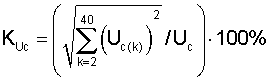
Consider the process of forming the input signal s in the control system 18 (the signal at the output of the adaptive controller). The output signal s c from the output of the input voltage sensor 1 is input to the meter 16 of the power line voltage form factor. At the output of the latter, a signal s kf is formed :
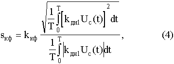
Where k kf is the conversion factor of the meter 16 of the power line voltage form factor;
K dn1 - transmission factor of the sensor 1 of the input voltage;
T is the period of oscillation of the input voltage of the network.
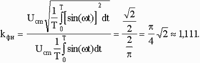
The input of the summing unit 17 receives signals corresponding to the actual value of the shape factor s kf, and the form factor setting signal s kphase corresponding to the undistorted form of the input alternating voltage. For an undistorted sinusoidal shape of the supply voltage, the shape factor k fn is [Measurements in electronics: Handbook / Ed. Kuznetsova V.A. - M .: Energoatomizdat, 1987. - 512 p., P.86 ] s kfzad = 1,111:
The adaptive controller 12 is an algorithmic block, the implementation of which involves the use of a microprocessor. Therefore, the process of functioning is considered further in discrete time at sampling times n-1, n, n + 1 ...
In the case where the measured network voltage waveform coefficient at the nth time moment s kf (n) differs from the form factor for the undistorted form of the supply voltage, an error signal is generated at the output of the summing unit 17 ![]() N = s кфзад -s кф(n) . Discrete error signal
N = s кфзад -s кф(n) . Discrete error signal ![]() N arrives at the input of the calculator 15. The calculator realizes the adjustment of the transmission coefficients (matrix W n ) of the adaptive filter by the method of least squares [Widrow B., Stearns C. Adaptive signal processing. M .: Radio and Communication, 1989. - 440 pp., P.94 ... 101]:
N arrives at the input of the calculator 15. The calculator realizes the adjustment of the transmission coefficients (matrix W n ) of the adaptive filter by the method of least squares [Widrow B., Stearns C. Adaptive signal processing. M .: Radio and Communication, 1989. - 440 pp., P.94 ... 101]:
![]()
Where S c (n) = [s c (n) s c (n-1) ... (s c (nL) ] T is the vector of the input signal of the adaptive filter 13;
L is the order of the adaptive filter 13;
![]() - coefficient determining the rate of adaptation of the method of least squares.
- coefficient determining the rate of adaptation of the method of least squares.
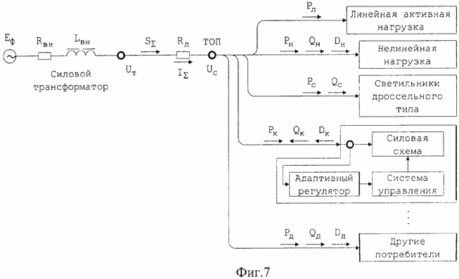
The change in the transmission coefficients W n results in the output signal u φ of the adaptive filter 13 being different from the sinusoidal one. The output signal u f of the adaptive filter 13 is fed to the input of the full-wave rectifier 14, which extracts the signal module u φ . The output signal of the full-wave rectifier 14 is fed to the input of the control system 18. Adjusting the transmission coefficients W n results in the form of the current being consumed becoming different from the sinusoidal one. As a result, higher harmonics of the current being consumed are injected into the supply network. At the next step of the iterative adjustment of the transmission factors, the process is repeated, which leads to a change in the shape of the supply voltage curve. The process of adaptive tuning is aimed at minimizing the error between the actual and the given shape of the voltage curve of the mains. Thus, the process closes through the influence of the claimed device on the shape of the supply voltage, and consequently, on the power quality indicators. During the tuning process, the level of harmonics injected into the supply network changes shape and tends to minimize the error of the error ![]() N between the given value of the form factor s kphase and the actual s kf (n) at the next (n + 1) th step of the adjustment. Let us explain the process of correction of the shape of the supply voltage curve for an example of a fragment of an alternating current network (Fig. 6).
N between the given value of the form factor s kphase and the actual s kf (n) at the next (n + 1) th step of the adjustment. Let us explain the process of correction of the shape of the supply voltage curve for an example of a fragment of an alternating current network (Fig. 6).
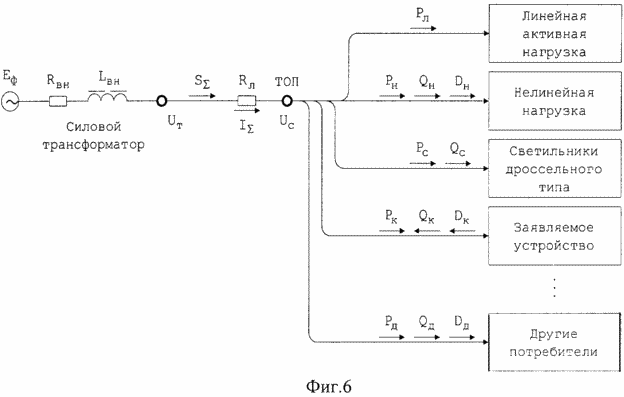
The power supply system under consideration includes a power transformer (or other source) with a phase emf. E ф and the active and reactive components of the internal resistance R вн and X вн (k) = k ![]() L вн (
L вн ( ![]() - the main frequency of the supply network curve; K is the harmonic number), the total power of which is commensurate with the total power of all consumers connected at the common connection point (TOP). It is understood that there is no distortion at the source of the phase distortion source, i.e. The amplitudes of the higher harmonics are zero. For simplicity, the communication line between the output of the power transformer and the TOP is represented by the active resistance R l . Consumers are represented (arrows reflect the direction of power transfer):
- the main frequency of the supply network curve; K is the harmonic number), the total power of which is commensurate with the total power of all consumers connected at the common connection point (TOP). It is understood that there is no distortion at the source of the phase distortion source, i.e. The amplitudes of the higher harmonics are zero. For simplicity, the communication line between the output of the power transformer and the TOP is represented by the active resistance R l . Consumers are represented (arrows reflect the direction of power transfer):
- linear load, consuming active P l power;
- non-linear load, consuming active P н , reactive Q n and power distortion D н ;
- lamps of throttle type, consuming active P s and reactive Q c power;
- the claimed device - a source of secondary power supply with distortion compensation in the supply network, consuming an active P to and generating a reactive Q to the network and a distortion power D k ;
- by other consumers consuming in the general case active RD, reactive QD and distortion power D e .
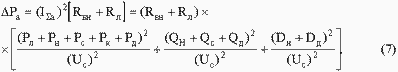
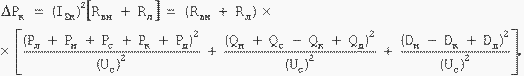
We estimate the technical and economic effect of using the proposed invention. To do this, we determine the total current consumed I ![]() A and loss of active
A and loss of active ![]() P a power in the TOP at operation of all consumers, provided that the claimed source of secondary power supply with distortion compensation in the power network consumes only the active power, i.e. Q k = 0 and D k = 0:
P a power in the TOP at operation of all consumers, provided that the claimed source of secondary power supply with distortion compensation in the power network consumes only the active power, i.e. Q k = 0 and D k = 0:
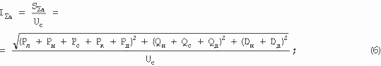
Let's write the expression for the instantaneous voltage value in TOP and TOP (t) as the difference between the instantaneous values of the phase voltage EF and the voltage drop of the total consumed current I ![]() A on the network elements:
A on the network elements:
![]()
Where E fm is the amplitude of the harmonic component of the voltage in the source circuit;
I m (k) is the amplitude of the k-th harmonic component of the current in the source circuit.
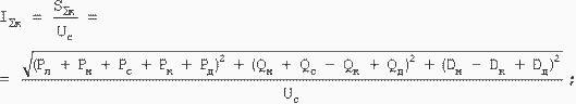
In this mode of operation, the voltage at the common connection point contains harmonic components, which are the consequence of the work of nonlinear loads. In this case, the shape of the voltage curve at the common attachment point will differ from the value determined for a purely sinusoidal curve. Let us estimate the total current consumption I ![]() K and loss of active
K and loss of active ![]() P to the power in the TOP in the operation of all consumers, provided that the declared source of the stabilized voltage with the distortion power compensation in the single-phase AC network consumes the active power, and in the power supply generates the reactive power Q to <0 and the distortion power D to <0:
P to the power in the TOP in the operation of all consumers, provided that the declared source of the stabilized voltage with the distortion power compensation in the single-phase AC network consumes the active power, and in the power supply generates the reactive power Q to <0 and the distortion power D to <0:
 (9)
(9)
 (10)
(10)
In the case under consideration, the shape of the supply voltage curve is close to the value for the sinusoidal shape. The adaptive tuning process is terminated by injecting higher harmonic components into the power network and explained in FIG.
The analysis of expressions (7) and (9) shows that injection into the supply network of current harmonics from the side of the secondary power supply declared by the source with compensation of distortions in the supply network allows to provide a positive effect in comparison with the prototype:
- Reduce the loss of active power in the power supply system: ![]() P to <
P to < ![]() P a ;
P a ;
- Compensate the inactive (reactive power and distortion power) of the total power component;
- improve the quality of electricity [GOST 13109-97. Electric Energy. Compatibility of technical means is electromagnetic. Norms of quality of electric energy in electrical networks of general purpose. - M .: Publishing house of standards, 1998. - 31 p.] Regarding the established deviation of stress ![]() U c : the value of voltage loss is reduced due to partial compensation of distortion power and reactive power of consumers;
U c : the value of voltage loss is reduced due to partial compensation of distortion power and reactive power of consumers;
- improve the quality of electricity [GOST 13109-97. Electric Energy. Compatibility of technical means is electromagnetic. Norms of quality of electric energy in electrical networks of general purpose. - М .: Publishing house of standards, 1998. - 31 p.] In the part of the distortion coefficient of the sinusoidal curve of the voltage
In TOP: the values of the higher harmonic components of the supply voltage curve are reduced due to partial compensation of the power distortion of consumers.
The meter 16 of the network voltage waveform factor implements the algorithm of integrated signal processing and can be performed on the analogue element base with the use of signal multipliers [Popov BC, Zhelbakov IN Measuring the rms voltage. - Moscow: Energoatomizdat, 1987. - 120 p .; Alexenko AG, Kolumbet EA, Starodub GI The use of precision analog ICs. - 2 ed., Pererab. And additional- M .: Radio and Communication, 1985. - 256 p.] Or on a digital algorithmic (software) block with digital signal processing [Gorlach AA, Mints M.Ya., Chinkov V.N. Digital signal processing in measuring technology. - Kiev: Technics, 1985., p.62 ... 68].
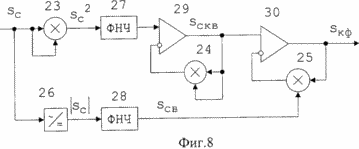 |
FIG. 8 shows an example of a technical implementation of the meter 16 of the power line voltage form factor on an analogue element base. It contains signal multipliers 23, 24, 25, a precision full-wave rectifier 26, low-pass filters 27, 28, operational amplifiers 29, 30. |
The investigated signal s c , whose shape factor is required to be determined, is fed to both inputs of the multiplier 23 and the precision full-wave rectifier 26. The output signals s with2 and | s with | From the outputs of the considered cascades go to the inputs of the low-pass filters 27 and 28, which allocate a constant component of the considered signals:
![]()
Where k 1 is the transmission coefficient of the multiplier 23;
K 3 is the transmission coefficient of the full-wave rectifier 26;
K 2 , k 4 are the transmission coefficients of the low-pass filters 27 and 28, respectively.
On the operational amplifier 29 and the multiplier 24, the square root extraction scheme is implemented:
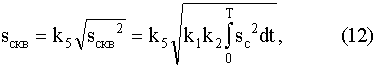
Where k 5 is the conversion coefficient of the square root extraction circuit based on the operational amplifier 29 and the multiplier 24.
The signals from the outputs of the operational amplifier 29 and the low-pass filter 28 are fed to the signal dividing circuit based on the operational amplifier 30 and the multiplier 25, where a signal proportional to the shape factor is generated:
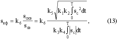
Where k 6 is the conversion factor of the signal dividing circuit based on the operational amplifier 30 and the multiplier 25.
Thus, at the output of the operational amplifier 30, a signal s kp is generated, proportional to the shape of the supply voltage curve of the network.
A variant of technical realization of a precision full-wave rectifier 26 is given in [Titze U., Shenk K. Semiconductor Circuitry: A Reference Guide. Trans. With him. - Moscow: Mir, 1982, 512 pp., P.471].
As a regulator 21, which is part of the control system 18, a proportional-integrating or integrating regulator can be used, the version of which is shown in [Titze U., Shenk K. Semiconductor Circuitry: A Reference Guide. Trans. With him. - Moscow: Mir, 1982, 512 pp., P.480 ... 484].
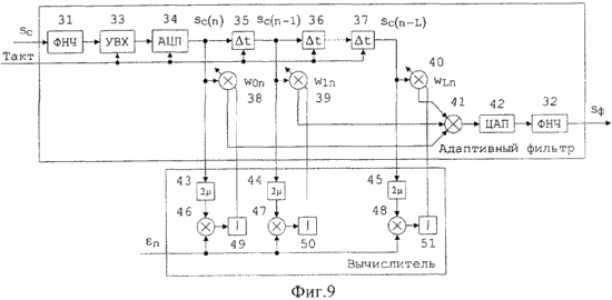
FIG. 9 shows an embodiment of an adaptive filter 13 and a calculator 15. An adaptive filter includes [Titze U., Shenk K. Semiconductor Circuitry: A Reference Guide. Trans. With him. - Moscow: Mir, 1982, 512 pp., P.425; Widrow B., Stirnz S. Adaptive signal processing. M .: Radio and Communication, 1989. - 440 p., P.96] low-pass filters 31 and 32, sampling-storage device 33, analog-to-digital converter 34 ADC, delay elements 35 ... 37, the number of which is determined by the order Adaptive filter L, multipliers 38 ... 40, the number of which is determined by the order of the adaptive filter L, the adder 41, the digital-to-analog converter 42 of the DAC.
The calculator 15 includes amplifiers 43 ... 45 with a transmission factor of 2 ![]() , Multipliers 46 ... 48 and integrators 49 ... 51.
, Multipliers 46 ... 48 and integrators 49 ... 51.
The input signal s c is filtered by the low-pass input filter 31, gated and stored by the storage sampling device 33, and digitized by the ADC 34. A time-shift ![]() T delay elements are made at the clock times, which are determined by the timing pulses on the input "Clock". At the output of the ADC 34 and delay elements 35 ... 37, discrete time signals s c (n) , s c (n-1) , s c (nL) are generated at the inputs of multipliers 38 ... 40, To the input of the adder 41. The output digital signal of the adder 41 is converted to an analog signal of the DAC 42, then it is filtered out by the low-pass filter 32. The output signal s φ of the latter is the output signal of the adaptive filter.
T delay elements are made at the clock times, which are determined by the timing pulses on the input "Clock". At the output of the ADC 34 and delay elements 35 ... 37, discrete time signals s c (n) , s c (n-1) , s c (nL) are generated at the inputs of multipliers 38 ... 40, To the input of the adder 41. The output digital signal of the adder 41 is converted to an analog signal of the DAC 42, then it is filtered out by the low-pass filter 32. The output signal s φ of the latter is the output signal of the adaptive filter.
The input signals of the calculator 15 are the samples of the input signal at discrete instants of time, s c (n) , s c (n-1) , s c (nL) , arriving at the inputs of the amplifiers 43 ... 45, and from them to the inputs of multipliers 46 ... 48. Integration of the output signals of the adder 46 ... 48 occurs in the integrators 49 ... 51, whose outputs form the output bus of the calculator, forming a vector of weights in the n-th step of the adaptive adaptive filter adaptation process.
Structurally adaptive filter and calculator is expedient to perform on the basis of microprocessors, equipped with an input analog-to-digital converter.
CLAIM
A source of secondary power supply with distortion compensation in the supply network, comprising an input voltage sensor, a bridge single-phase diode rectifier, a current sensor, an output voltage sensor, a load, a control system comprising a comparator, a multiplier, a controller and an adder; A diode, a cut-off diode, a power transistor, a smoothing capacitor and a driver device, the input of a bridge single-phase diode rectifier being the input of a secondary power supply source with distortion compensation in the supply network, and an input voltage sensor is connected to this input, the upper output of a bridge single-phase diode rectifier is connected to The upper input of the DC voltage impulse converter, and the lower one through the current sensor is connected to the lower input of the up-converter DC voltage transducer, and to the outputs of the latter is connected the output voltage sensor and the load, the outputs of the current sensor and the output voltage sensor are respectively connected to the second and third inputs And the first input of the control system is connected to the first input of the multiplier whose output is connected to the non-inverting input of the comparator, the second input of the control system is connected to the inverting input of the comparator, the output of the comparator is the output of the control system and carries out switching of the DC- The fourth inputs of the control system are connected respectively with the subtracting and summing inputs of the adder, the output of the latter through the series-connected controller is connected to the second input of the multiplier, and the fourth input of the control system is supplied with a driving signal, characterized in that an adaptive controller is introduced therein, The first input of the adaptive controller is connected to a point combining the input of the adaptive filter, the first input of the calculator and the input of the meter of the voltage-form factor of the supply voltage Network, and the output of the adaptive filter through a series-connected full-wave rectifier is connected to the first input of the control system, the subtracting input of the summation unit is connected to the output of the meter of the voltage-form of the supply network, and the summation input of the summing unit is fed with the network voltage form factor setting signal, Is connected to the second input of the calculator, the output bus of which is connected to the input bus of the adaptive filter.
print version
Published on February 15, 2007
![]()

Comments
When commenting on, remember that the content and tone of your message can hurt the feelings of real people, show respect and tolerance to your interlocutors even if you do not share their opinion, your behavior in the conditions of freedom of expression and anonymity provided by the Internet, changes Not only virtual, but also the real world. All comments are hidden from the index, spam is controlled.