| Start of section
Production, amateur Radio amateurs Aircraft model, rocket-model Useful, entertaining |
Stealth Master
Electronics Physics Technologies Inventions |
Secrets of the cosmos
Secrets of the Earth Secrets of the Ocean Tricks Map of section |
  |
| Use of the site materials is allowed subject to the link (for websites - hyperlinks) | |||
Navigation: => |
Home / Patent catalog / Catalog section / Back / |
|
INVENTION
Patent of the Russian Federation RU2278459
![]()
QUASI-RESONANT HIGH-FREQUENCY VOLTAGE TRANSDUCER
The name of the inventor: Goryashin Nikolai Nikolaevich (RU); Lukyanenko Mikhail Vasilyevich (RU); Bazilevsky Alexander Borisovich
The name of the patent holder: Goryashin Nikolai Nikolaevich (RU); Lukyanenko Mikhail Vasilyevich (RU); Bazilevsky Alexander Borisovich
Address for correspondence: 660014, Krasnoyarsk, Krasnoyarskiy worker, 48, ap. 11, ABBazilevsky
Date of commencement of the patent: 2004.12.08
The invention relates to converter technology and can find application in autonomous power supply systems, in particular in secondary power supplies with transformerless output. The voltage converter comprises a key element in the circuit of a series-connected resonant inductor, one terminal of which is connected to the output of the key element and the other to the potential overlap of the capacitor of the resonant circuit connected to the cathode of the inverse regenerative diode and the output of the output filter coil, the other terminal of which is connected With the potential overlap of the output filter capacitor, and the regenerative diode anode and other plates of the capacitors of the resonant circuit and the output filter are combined and connected to the common converter bus. The voltage converter input is connected to the primary power source (PIE), and the output to the load resistance (Rn). New in the device is that the key element is made in the form of two counter-series-connected power MOSFETs in such a way that their common point is the source, and the control signal is fed between a common point and interconnected gates. The technical result: increase in efficiency and specific power.
DESCRIPTION OF THE INVENTION
The present invention relates to converter technology and can find application in autonomous power supply systems, in particular in secondary power supplies with transformer-free output.
Known devices of a similar purpose are voltage converters (PN) with a rectangular shape of voltage and current [Dyakonov VP, Maksimchuk AA Encyclopedia of devices on field transistors. M .: SOLON - R. 2002. p.512., Switched-Mode Power Supply Design Manual VeriBest, inc. The EDA Systems Company] to the disadvantages of which include: the inability to improve the energy performance without increasing the speed of key elements (CE), reducing the voltage drop on the CE in the open state. This tendency enhances the influence of the parasitic reactive components of the real circuit, i.e. With an increase in the rate of change in the voltage at the collector (sink), the amplitude of the signal at higher harmonics increases, the frequencies of which can coincide with the natural frequencies of the resonant circuits formed by the parasitic elements of the circuit, which leads to an increase in high-frequency noise imposed on the output voltage of the converter.
Of the known devices, the closest in terms of their technical nature to the claimed one is the quasiresonant PN [RWErickson Fundamentals of Power Electronics First Edition: Chapman and Hall, May 1997. 791 pages, 929 line illustrations.] And accepted for the prototype. This PN contains the CE, implemented on a single power field-effect transistor, connected in series between the primary power source (PIE) and the circuit comprising a series-connected diode, a resonant circuit (RC) containing a resonance inductor Lp, one of the leads of which is connected to the cathode Pass diode, and the other terminal to the resonant capacitor Cp, in parallel to which the switched-back recuperative diode is connected, to the cathode of which the output LφCφ-filter is connected.
The main disadvantage of this prototype is the presence of a circulating diode in the FE circuit, and as a result, an increase in power losses and a limitation of the switching frequency. The presence of a circulating diode is justified in that it prevents reverse current through the parasitic diode of a power MOS transistor, which can be caused by an ongoing resonance process. This prevents the return of energy accumulated in the resonant circuit back to the PIE. A common drawback of powerful high-speed diodes is the relatively longer reverse recovery time, during which it acts as a capacitor, and a significant direct voltage drop that is non-linearly dependent on current and temperature.
The task, to solve which the claimed invention is directed, is reduction of losses in the CE with simultaneous increase in the switching frequency, due to which the efficiency is increased and the specific power is increased.
The problem is solved by the fact that a quasi-resonant high-frequency voltage converter (CVT) contains a key element in the circuit of a series-connected resonant inductor, one terminal of which is connected to the output of the key element, and the other to the potential overlay of the resonant circuit capacitor connected to the cathode of the reverse-shifted recuperative diode And output of the inductor of the output filter, the other terminal of which is connected to the potential overlap of the output filter capacitor, and the anode of the regenerative diode and other plates of the capacitors of the resonant circuit and the output filter are combined and connected to the common bus of the converter. The voltage converter input is connected to the primary power source (PIE), and the output to the load resistance (Rn). New in the device is that the key element is made in the form of two counter-series-connected power MOSFETs in such a way that their common point is the source, and the control signal is fed between a common point and interconnected gates.
 |
 |
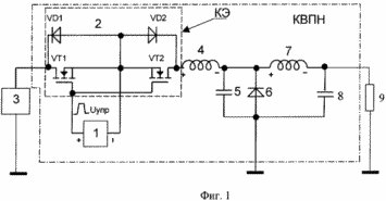
1 is a schematic diagram of the claimed device. |
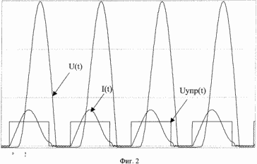
FIG. 2 shows timing diagrams of operation. FIG. |
The claimed device consists of a control unit 1 whose output is connected to the input of a key element 2 consisting of two counter-series-connected power MOSFETs VT1, VT2 in such a way that the parasitic diodes VD1, VD2 are turned on and off, and their anodes are connected to a common Point. The cathode of the diode VD1 is connected to the potential bus of the primary power source 3, the cathode of the diode VD2 is connected to one of the terminals of the resonant inductor Lp 4, the other terminal of which is connected to the potential overlap of the resonant capacitor Cp 5. Parallel Cp 5 includes a reversed recuperative diode 6, One of the inductances of the output filter coil Lf 7 is connected, and to the other terminal Lf 7 the potential overlap of the output filter capacitor Cf 8 is connected. In parallel with the capacitor Сф 8, the load resistance Rn 9 is connected. The anode of the recuperative diode 6 and other plates of capacitors of the resonant circuit Cp5 and output Filter cp 8 are combined and connected to the common bus of the converter.
Initially, the transistors VT1, VT2 are closed. The output current flows due to the energy stored in the inductance coil of the output filter 7. At some time, determined by the control device 1, the FE 2 opens. The oscillatory circuit formed by the resonant inductor Lp 4 and the capacitor Cp 5 begins to receive energy from the PIE 3. The charge of the capacitor Cp5 and its subsequent discharge will occur according to a law close to the sinusoidal frequency with a frequency equal to the resonant frequency of the LpCp 4.5 loop. Simultaneously, the current in the inductor Lp 4 and will vary according to the sinusoidal law - first increase, then decrease. When this current decreases to zero, the CE 2 locks. In this case, the back-and-forth diodes VD1, VD2 prevent the reverse current, which could be caused by the ongoing resonance process.
When the current in the inductor Lp 4 becomes zero, the output current flows through the inductor coil of the output filter Lf 7 and the capacitor Cp 5, which is rapidly discharged. As soon as it is discharged to zero, diode 6 opens. At this one resonant cycle ends.
When a signal is sent to the gates of power MOSFETs, they are unlocked, where the duty cycle and the switching frequency are determined by the known control law [L. K. Wong, Frank H. Leung, Peter K. S. Tarn. A Simple Large-Signal Nonlinear Modeling Approach for Fast Simulation of Zero-Current-Switch Quasi-Resonant Converters. IEEE Trans. Power Electron., Vol. 12, no. 3, p.437-442, may 1997, J. Abu-Qahouq and I. Batarseh, Unified Steady-State Analysis of Soft-Switching DC-DC Converters, IEEE Trans. Power Electron., Vol.17, no. 5, pp. 684-691, sep. 2002], the meander at the output of the Uynp (t) control unit 1 in Fig. 2, the current in Lp 4 I (t), and the voltage at Cp 5 U (t).
Reduction of losses in the claimed KVPN, in contrast to the prototype, in which the FE is performed on a single power transistor and a diode connected in series, is achieved by performing the CE in the form of a spirit of interconnected-series MOS transistors having, in comparison with the gate diode, As a large speed, and a lower voltage drop. In this case, the requirements for the speed of the CE can be lowered, which makes it possible to use a pair of MOSFETs with a minimum resistance of the open channel with an allowable drain-source voltage, thereby reducing losses and achieving high efficiency at a high specific power.
CLAIM
A quasiresonant high-frequency voltage converter comprising a key element in the circuit of a series-connected resonant inductor, one terminal of which is connected to the output of the key element, and the other to the potential overlap of the capacitor of the resonance circuit, connected to the cathode of the back-biased regenerative diode and outputting the output filter coil, The other terminal of which is connected to the potential overlap of the output filter capacitor, and the anode of the recuperative diode and the other plates of the capacitors of the resonance circuit and the output filter are combined and connected to the common bus of the converter, characterized in that the key element is made in the form of two counter-series-connected power MOSFETs So that their common point is the source, and the control signal is supplied between the common point and interconnected gates.
print version
Publication date 17.02.2007gg
![]()

Comments
When commenting on, remember that the content and tone of your message can hurt the feelings of real people, show respect and tolerance to your interlocutors even if you do not share their opinion, your behavior in the conditions of freedom of expression and anonymity provided by the Internet, changes Not only virtual, but also the real world. All comments are hidden from the index, spam is controlled.