
| Start of section
Production, amateur Radio amateurs Aircraft model, rocket-model Useful, entertaining |
Stealth Master
Electronics Physics Technologies Inventions |
Secrets of the cosmos
Secrets of the Earth Secrets of the Ocean Tricks Map of section |
  |
| Use of the site materials is allowed subject to the link (for websites - hyperlinks) | |||
Navigation: => |
Home / Patent catalog / Catalog section / Back / |
|
INVENTION
Patent of the Russian Federation RU2284639
![]()
INVERTER VOLTAGE
The name of the inventor: Banin Roman Valerievich (RU); Kutepov Vladimir Nikolaevich
The name of the patent owner: Federal State Educational Institution of Higher Professional Education "Chelyabinsk State Agroengineering University"
Address for correspondence: 454080, Chelyabinsk, Lenin Ave., 75, Chelyabinsk State Agroengineering University, Department "Electrical Machines and Operation of Electrical Equipment in Agriculture"
Date of commencement of the patent: 2005.06.29
The invention relates to the field of electrical engineering and can be used for autonomous power supply to consumers by converting the voltage of a direct current source into an alternating one. SUMMARY OF THE INVENTION: the circuit comprises a clock generator, an inverter startup unit, a power filter, switching transistors, a step-up transformer. The power input of the clock generator elements is connected to the output of the power filter, the input connected to the DC source, and its positive pole is connected to the middle point of the primary winding of the step-up transformer, parallel to the secondary winding of which the smoothing capacitor is turned on. The leads of the primary winding of the step-up transformer are connected to the corresponding outputs of the first and second commuting transistors, the inputs connected to each other. As the first and second commutating transistors, field-effect transistors are used, the drains of which are connected to the negative pole of the DC source via a parallel-connected additional resistor and a shunt contact of the intermediate relay. A start-up unit is installed that allows to provide a technical result - to expand the functionality of the voltage inverter, to increase the reliability of the voltage inverter during start-up and (or) failures in the power supply. The use of field-effect transistors as commutators increased the overload capability of the voltage inverter, its efficiency, reduced the drift of the output voltage, and improved the weight and dimensions.
DESCRIPTION OF THE INVENTION
The invention relates to the field of electrical engineering and can be used in industry and agriculture for autonomous power supply to consumers by converting the voltage of a direct current source into an alternating voltage.
A voltage converter known in the literature is known (see I.Nechaev, Voltage converter 12/220 V 50 Hz // Radio, 2004. - No. 9, p.30-31), in which there is a clock generator, a power filter , Power amplifier, step-up transformer and current overload protection relay.
The converter provides inverting the voltage of a direct current source to an alternating voltage of 220 V with a frequency of 50 Hz.
Disadvantages of the converter are:
- low efficiency due to a significant voltage drop in the winding of the current relay;
- the complexity of implementing the converter circuit due to the use of a specialized chip clock generator and current relay special manufacture;
- low reliability of the circuit due to the large number of elements and the absence of a current-limiting resistor at the outputs of the clock generator; In the breakdown of commuting transistors, the chip of the clock generator breaks down.
The closest in technical essence and achieved effect to the proposed technical solution is the voltage converter published in the literature (see S.Karlashchuk, V.Karlashchuk, Transducer for electric shavers // Radio, 1989. - No. 11, p.69), A clock generator comprising a master oscillator and a frequency divider, a power filter, a preamplifier, a power amplifier, and a step-up transformer.
The converter provides inverting the DC voltage of 12 V to the AC voltage with an effective value of 220 V at a frequency of 50 Hz.
Disadvantages of this converter are:
- Limited functionality due to low power output, which is prevented by significant overvoltages that occur in the transistors of the power amplifier when the power is turned on. In this connection, during design, transistors with a significantly overestimated operating voltage are selected, which leads to a decrease in the rated output current of these elements;
- low reliability, due to the lack of protection of switching transistors of the power amplifier from overvoltages when switching on or short-term power failure;
- low overload capacity and short-circuit resistance;
- low efficiency, associated with significant switching losses in the transistors of the power amplifier;
- significant drift of the output voltage, caused by a change in the resistance of commuting transistors depending on the load;
- Significant weight and dimensions.
It is an object of the present invention to expand the functionality of the converter, increase its reliability, overload capability, short-circuit resistance, increase efficiency, improve output voltage stability, and improve mass-dimensions.
The task is solved by a voltage inverter comprising a master oscillator and a frequency divider that form a clock generator, the input of the latter's power supply is connected to the negative pole of the DC source connected to the common power filter wire by one terminal and connected to the output of the power filter, With the positive pole of the direct current source, with the positive pole of the constant current source and connected to the middle point of the primary winding of the step-up transformer parallel to the secondary winding of which the smoothing capacitor is turned on, and the terminals of the primary winding of the step-up transformer are connected to the corresponding inputs of the first and second switching transistors, the outputs connected between By means of the installation of a voltage inverter starting unit with an intermediate relay, the coil of which is connected to the output of the power filter connected to each other, the cathode of the protective diode and the first terminals of the discharge resistor and the time-setting capacitor, and their second terminals are connected to the input of the logic element and The first terminal of the time-setting resistor, the second terminal of the control-connected transistor connected to the drain, and the negative pole of the DC source, wherein the other terminal of the intermediate relay coil is connected to the anode of the protective diode and the source of the control transistor, and the gate of the control transistor is connected to the output of the logic element through the current-limiting resistor, The power input of the logic element is connected by one wire to the negative pole of the DC source, while the other wire is connected to the output of the power filter. Field transistors are used as the first and second switching transistors. The gate of the switching transistors are connected directly to the first and second outputs of the clock generator, and the drain of the transistors is connected to the negative pole of the DC power source through a parallel-connected additional resistor and a shunt contact of the intermediate relay.
This allowed to expand the functionality of the inverter by increasing the output power by installing the voltage inverter starting unit. The efficiency of the inverter has increased, the stability of the output voltage has improved, the reliability of the inverter has improved and its weight and size parameters have been improved by simplifying the design of the power amplifier and installing field-effect transistors as commutators.
According to the information available to the authors, the set of essential features characterizing the essence of the claimed invention is not known from the state of the art, which makes it possible to conclude that the invention meets the "novelty" criterion.
According to the authors, despite the fact that the elements making up the voltage inverter are known in the art, but a new set of features, namely, the installation of field-effect transistors as commutators and a start-up unit, their interconnection and properties, which in this case appear to allow obtaining such a Technical result, such as simplifying the design, increasing the output power, reliability, overload capacity, short circuit resistance, increasing the efficiency of the inverter, stability of the output voltage, improving the weight and size parameters are not known and do not follow explicitly from the prior art; The causal relationship of the above mentioned signs and the received technical result was not known, which makes it possible to conclude that the technical solution corresponds to the criterion "inventive level".
The set of essential features characterizing the essence of the invention can in principle be reused in industry and agriculture with the obtaining of a technical result consisting in increasing the output power of the voltage inverter, which ensures the achievement of the set goal - the expansion of the functionality of the voltage inverter, On the compliance of the invention with the criterion "industrial applicability".
The essence of the invention is explained by the drawing, which shows the principal circuitry of the voltage inverter.
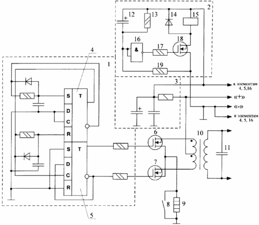
The voltage inverter comprises a clock generator 1 formed by a master oscillator 4 and a frequency divider 5 combined in a CMOS dual-D flip-flop chip. The power input of the clock generator 1 is connected in one terminal to the negative pole of the DC power source connected to the common wire of the power filter 3, and the other terminal is connected to the output of the power filter 3, the input of the DC source connected to the positive pole, with the positive pole of the DC source and Is connected to the middle point of the primary winding of the step-up transformer 10, in parallel with the secondary winding of which a smoothing capacitor 11 is connected. The terminals of the primary winding of the step-up transformer 10 are connected to the respective inputs of the first and second commutating transistors 6, 7 connected with each other. And as the inputs of commuting transistors 6, 7 their sources are used, and the sinks of these transistors are their outputs. In addition, a voltage inverter starting unit 2 is installed with an intermediate relay whose coil 15 is connected to the output of the power filter 3 connected to each other, the cathode of the protection diode 14 and the first terminals of the discharge resistor 13 and the time-consuming capacitor 12, and their second terminals are connected to the input The logic element 16 and the first terminal of the time-setting resistor 19, the second terminal of the drain-bound control transistor 18 and the negative pole of the DC source. The other terminal of the intermediate relay coil 15 is connected to the anode of the protection diode 14 and the source of the control transistor 18. The gate of the control transistor 18 is connected to the output of the logic element 16 via a current limiting resistor 17. The power input of the logic element 16 is connected to the negative pole of the DC source by one wire The other wire is connected to the output of the power filter 3. As the first and second switching transistors 6, 7, field effect transistors are used, the gate of which is connected directly to the first and second outputs of the clock generator 1, and the drains of the first and second switching transistors 6, 7 are connected to the negative Pole of the DC power supply via a parallel connected to each other, an additional resistor 9 and a shunt contact 8 of the intermediate relay.
INVERTER WORKS AS FOLLOWS:
When connected to a direct current source, a clock pulse generator is fed from the output of the power filter 3. On the first and second outputs of the clock generator 1, rectangular pulses of 50 Hz frequency appear alternately.
From the first output of the clock generator, the control signal is applied to the gate of the first switching transistor 6. The transistor opens. The current flows from the positive pole of the DC source through one of the windings of the primary winding of the step-up transformer 10, the first switching transistor 6 and the additional resistor 9 to the negative pole of the DC source. Then, the control pulse on the gate of the first switching transistor 6 disappears. This results in the closure of the first switching transistor 6 and the termination of the current through the half-winding.
The next control pulse appears on the second output of the clock generator 1 and enters the gate of the second switching transistor 7. The transistor opens. The current flows from the positive pole of the DC source through the other half-winding of the step-up transformer 10, the second switching transistor 7 and the additional resistor 9 to the negative pole of the DC source.
As a result, an alternating voltage appears on the secondary winding of the step-up transformer. To approximate the shape of the output voltage to the sine wave, a smoothing capacitor 11 serves.
Then the described process is cyclically repeated, beginning with the appearance of a control pulse on the first output of the clock generator 1.
It should be noted that at the moment of starting with an open shunt contact 8 of the intermediate relay, a voltage drop is created on the additional resistor 9, which ensures safe start of the inverter.
Simultaneously with the start of the clock pulse generator 1, the startup unit 2 of the voltage inverter is supplied. The time-consuming capacitor 12 begins to charge. The charging current flows from the positive pole of the DC source through the power filter 3 and the time-setting resistor 19 to the negative pole of the DC source. The input potential of the logic element 16 begins to increase as the time-consuming capacitor 12 is charged. When a certain level is reached, the logic element 16 opens. A voltage corresponding to the state of the logical unit appears on its output and is fed through the current-limiting resistor 17 to the gate of the control transistor 18. It opens and supplies voltage to the intermediate relay coil 15. The relay trips and closes the auxiliary resistor 9 by a shunt contact 8. The voltage inverter goes to the nominal operating mode.
When the power is turned off and on again, or if it is temporarily lost, the logic element 16 closes, de-energizing the intermediate relay coil 15. This is ensured by a fast discharge of the time-consuming capacitor 12 to the discharge resistor 13. Thus, the voltage inverter is restarted at a certain delay with the intermediate relay contact 8 open. This ensures the safety of starting the voltage inverter due to a voltage drop across the additional resistor 9, which reduces the overvoltage in the first and second commutating transistors.
Thanks to the installation of the start-up unit, the functionality of the voltage inverter has been expanded and its reliability has increased. The installed start-up unit allows increasing the output power and increasing the reliability of the voltage inverter during start-up and / or power failure.
The installation of field-effect transistors as commutation allowed to increase the overload capacity of the voltage inverter, its efficiency, and reduce the drift of the output voltage. In addition, weight and size indicators have improved.
CLAIM
A voltage inverter comprising a master oscillator and a frequency divider that form a clock generator is connected to the negative pole of the DC power source connected to the common wire by the power filter, and the other terminal is connected to the output of the power filter, the input connected to the positive pole of the source The positive pole of the constant current source and is connected to the middle point of the primary winding of the step-up transformer parallel to the secondary winding of which a smoothing capacitor is connected and the terminals of the primary winding of the step-up transformer are connected to the corresponding inputs of the first and second switching transistors, the outputs connected together, , That the startup unit of the voltage inverter is installed with an intermediate relay, the coil of which is connected to the output of the power filter connected to each other, the cathode of the protective diode and the first terminals of the discharge resistor and the time-setting capacitor, and their second terminals are connected to the input of the logic element and the first output of the time-setting resistor , The second terminal of the drain-connected control transistor and the negative pole of the DC source, the other terminal of the intermediate relay coil being connected to the anode of the protective diode and the source of the control transistor, and the gate of the control transistor is connected to the output of the logic element through the current-limiting resistor, Is connected by one wire to the negative pole of the DC source, the other wire is connected to the output of the power filter, and as the first and second switching transistors, field-effect transistors are used, the gate of which is connected directly to the first and second outputs of the clock generator, the drains of the first and second commuting Transistors are connected to the negative pole of a direct current source through a parallel-connected additional resistor and a shunt contact of the intermediate relay.
print version
Publication date 17.02.2007gg
![]()

Comments
When commenting on, remember that the content and tone of your message can hurt the feelings of real people, show respect and tolerance to your interlocutors even if you do not share their opinion, your behavior in the conditions of freedom of expression and anonymity provided by the Internet, changes Not only virtual, but also the real world. All comments are hidden from the index, spam is controlled.