
Development of LVDS signal transmission technology
The amount of data transferred is gigabit, consumption is milliwatts
Introduction
The Low Voltage Differential Signaling (LVDS) standard is today the best solution for systems with high-speed low-consumption interfaces. When using LVDS, high speed of exchange is achieved with low power consumption. Additional advantages are compatibility with low voltage power supplies, low interference and reliable signal transmission. For these reasons, this standard is widely used in manufacturing, in different market segments where speed and low consumption are required. Typical applications of this standard are connection of boards and cables in commutation switches, routers, industrial cameras, as well as in car entertainment and vehicle control systems. Even with all these advantages, there are some limitations on the use in devices that require support for multiple transceivers on the same bus, power from a low voltage bus, and receivers with an extended common-mode range. This led to the emergence of new LVDS standards, complementing the original standard.
The standard for the transmission of low-voltage differential signals (LVDS)
In 1994, National Semiconductor first introduced the technology of low-voltage differential signal (LVDS) transmission as a standard interface. Bandwidth requirements increased exponentially, and system developers were looking for ways to reduce power losses. Normal standards, such as RS-422 and RS-485, lacked speed, while ECL (emitter-coupled logic circuits) and CML (logic circuits with current switches) had a sufficient exchange rate, but consumed too much power. LVDS technology has helped to solve this problem without any compromise. This is a differential technology, that is, it uses two lines to transmit the signal (Figure 1). In addition, when using LVDS, a signal is transmitted with a current loop, while the logic level (high or low) is determined by the current direction in the loop (clockwise or counterclockwise). Approximately 3.5 mA goes by one pair wire and returns in another. A matching resistor produces a voltage (about ± 3.5 mA x 100 Ω = ± 350 mV). The receiver, the differential comparator, determines the polarity of the voltage drop, while the positive voltage value corresponds to a high level of logic, the negative value to a low value. The driver provides 350 mV of differential voltage at the output centered at about +1.25 V. The trigger threshold of the receiver is set to 100 mV with an input range of 0 to +2.4 V. This allows the nominal active signal to shift downward or upward by 1 V in In-phase mode due to the difference in ground potentials. The driver is designed for use with a load of 100 ohms, with a matching resistor of 100 ohms.
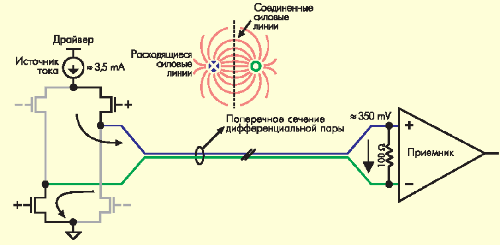
Figure 1. A simplified LVDS driver and receiver circuit connected via a carrier with a differential impedance of 100 ohm
The differential concept leads to a high gain in the form of common-mode rejection. Due to the high noise resistance, the signal amplitude can be reduced to only a few hundred millivolts. The smaller amplitude allows data to be exchanged faster, since the rise and fall of the signal is well monitored and held within 1 V / ns. A relatively constant small output current reduces background noise and power noise. Since the current in the transmitting pair is a closely related current loop, the electric scattering fields often disappear, reducing electromagnetic interference. The exchange rate varies depending on each individual device, but in any case it is within 1.5 Gb / s at a constant current. Power is minimized in three ways. The load current is limited to 3.5 mA, the current mode driver usually limits the dissipation of dynamic power, and the quiescent current is reduced to a minimum by CMOS processes at the submicron level. The transmission of low-voltage differential signals (LVDS) is defined in the ANSI / TIA / EIA-644-A-2001 standard, which is an update to the 1995 ANSI / TIA / EIA-644 standard. This standard specifies only the levels of LVDS electrical signals, that is, the driver output and receiver input characteristics. This standard must be applied together with other standards that define the complete interface, including protocol, connections and media. These are standards such as Camera Link or the FPD interface standard for laptops defined by the SPWG (Working Group of standard consoles), it is also used in many special applications. In addition, there are other standards. In Fig. 2 shows the amplitudes of the signals and the bias voltage (respectively) of the various LVDS standards.
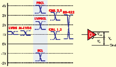
Figure 2. Oscillation of differential signals and comparison of displacement
To date, LVDS-crystals and sets of crystals with many functions are offered by several companies. In addition to simple linear drivers and receivers that perform the conversion between the LVDS and LVTTL levels, there are LVDS-LVDS buffers, coordinate switches, signal distributors (splitters) and clock distribution devices.
Particularly interesting are the sets of crystals for the transformation from parallel to serial and vice versa (SerDes), as they increase the speed of LVDS, which gives a great advantage to the whole system. LVDS technology provides the ability to integrate I / O with additional schemes such as: PLL (phase-locked loop) scheme for converting from parallel to serial form; With a register latch and even with digital circuits, for example with a test port of the Boundary SCAN Test Access Port. In Fig. 3 shows an example of a similar set of SerDes crystals. The serial-to-serial converter SCAN92LV1025 collects 10 slow input signals from TTL circuits and serializes them into a single high-speed LVDS channel.
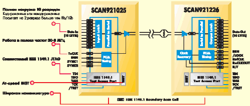
Figure 3. LVDS parallel-to-serial converter / serial-to-parallel converter with JTAG test added
Transmitter timing signals are embedded in a serial data stream by marking data with the start (HIGH) and stop (LOW) bits. The narrow LVDS interface does not require the use of multiple contacts, bulky heavy connectors and cables, which in turn reduces the cost of the system. The serial-to-parallel converter SCAN92LV1226 receives the LVDS signal, extracts the synchronization signal from the data stream and creates a 10-bit TTL bus. The bandwidth of this crystal can reach 800 Mbit / s of useful information. Such technical solutions SerDes are ideal for those systems where it is necessary to use fine wiring, for example, connection of video sensors in automobile chassis, manipulators, connections to measuring heads in automatic inspection equipment, etc. There are some limitations of LVDS, such as a common-mode signal of ± 1 V and a final load of 100 Ω. This caused several variations of the LVDS 1 standard.
1) For example:
- Standard ANSI / TIA / EIA-644 LVDS.
- Standard ANSI / TIA / EIA-644-A LVDS.
- Standard ANSI / TIA / EIA-899 M-LVDS.
- Specification of JEDEC GLVDS, version 1.0.
- JEDEC SLVS (JESD8-13) October 2001.
Bus Topology
First of all, LVDS is used in special high-speed point-to-point connections. The driver needs alignment with the line, and the connection parameters must be selected based on the characteristic input resistance of the cable. Due to this, high quality of signal transmission is achieved, and its reflection and radiation are minimized. To explain the difference between LVDS technology implementation options, it is necessary to recall the basic configurations of tires, the various designs of which are shown in Fig. 4. The simplest is a unidirectional bus with two dots, at the end of the cable there is only one termination resistor, and the driver is always on the opposite end of the cable. Due to high noise immunity, the point-to-point configuration supports high data rates. This bus structure makes it easy to create gigabit networks. In this case, for a bi-directional data transfer it is necessary to select a separate line (2 pairs). In this case, temporary transmission of data in two directions can be carried out, and the capacity of the common bus is doubled.
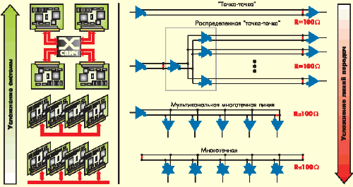
Figure 4. Different bus topologies
Another common configuration is a classical distribution system or a multi-point bus. The use of this configuration is especially effective if you need to transfer the same information to several points at once. As in the previous case, the driver is located on one end of the bus, and the terminating resistor is on the other. Along the tire there are two or more receivers with small connecting wires. The electrical length of these wires should be as low as possible in order to prevent the signal quality from deteriorating due to reflection, interference, etc. The exchange rate when using multipoint buses can reach 400-600 Mbit / s, depending on the connecting wires and load. The most flexible configuration is a multi-point bus with matching on both ends of the connecting wire. The driver can be anywhere on the bus. The operation of several drivers is simultaneously impossible, so the data transfer is two-sided, half-duplex. Connecting network nodes to the bus can be critical, so it should be done carefully. For systems with two termination resistors, so-called multi-point systems, more powerful drivers are needed to create oscillations like LVDS, while the load varies in the range of 30 to 50 ohms.
Derived LVDS
The table shows the main parameters of some varieties of LVDS.
Table 1. LVDS Comparison Table
| Parameter | LVDS | BLVDS | M-LVDS | GLVDS | LVDM |
| Amplitude at the output | 250 - 450 mV | 240 - 500 mV | 480 - 650 mV | 150 - 500 mV | 247 - 454 mV |
| Bias voltage | 1.125V | 1.3 V | 0.3 - 2.1 V | 75 - 250 mV | 1.125V |
| Completion | 100 W | 27 - 50 W | 50 W | Internal to RX | 50 W |
| Excitation current | 2.5 - 4.5 mA | 9 to 17 mA | 9 - 13 mA | Adjustable | 6 mA |
| Short-circuit current | <24 mA | <65 mA | <43 mA | - | -10 mA |
| Thresholds | ± 100 mV | ± 100 mV | ± 50 mV | ± 100 mV | ± 100 mV |
| Input voltage | 0 to +2.4 V | 0 to +2.4 V | -1,4 to +3,8 V | -0.5 to +1 V | 0 to +2.4 V |
| In-phase mode | ± 1V | ± 1V | ± 2V | ± 0.5 V | ± 1V |
LVDS bus
In 1997, National Semiconductor introduced the LVDS bus for controlling boards with high load and low input impedance. Cards with a large number of cards (up to 20 pieces) in a small space usually have an input resistance within 50-60 ohms. When matching at both ends in size, for example, 54 ohms the driver actually encounters a load of 27 ohms. To obtain the LVDS amplitudes, the driver output current must be tripled to a range of 10-12 mA. Another improvement of this technology was the matching of the overall output impedances of the driver, as well as the technology of preventing the simultaneous use of one channel. If several drivers try to access the bus at the same time, the output current will be lowered so as not to damage the I / O devices.
M-LVDS
A newer version of LVDS is the ANSI / TIA / EIA-899 standard, known as M-LVDS (Multipoint-LVDS). This version supports a multipoint bus with double matching and can use up to 32 nodes. M-LVDS also extends the common-mode range to ± 2 V. The maximum communication speed is 500 Mbps. In practice, the speed is limited to 300-400 Mbit / s depending on various parameters, for example, the length of the connecting wire and the required signal quality. M-LVDS has an output current of 9-13 mA and is applied to both the cable and the board connections. When using long cables, the likelihood of a large difference between ground potentials will increase. Thus, the M-LVDS standard doubled the range of the in-phase LVDS mode to ± 2 V for greater stability. M-LVDS also distinguishes two types of receivers (Figure 5). Type 1, called the "data receiver", has thresholds of ± 50 mV with a conventional hysteresis of 30 mV. Type 2 or "control receiver" switches the output to LOW when the input voltage drops below 50 mV. The output switches to HIGH at an input voltage higher than 150 mV. The advantage of shifting the threshold region by +50 mV is the appearance of a 50 mV noise margin.
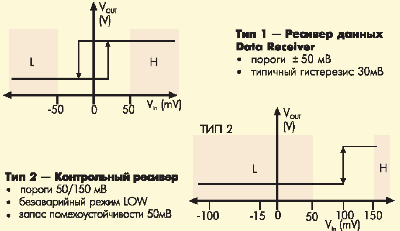
Figure 5. M-LVDS Type 1 and Type 2 Receiver
The outputs in this case are switched to the LOW position (trouble-free mode). By the way, M-LVDS was chosen by PICMG (PCI group for manufacturing computers for industry) as a signal transmission standard for the distribution of clock signals in ATCA compatible data transmission systems (ATCA - modern computer architecture for telecommunications).
GLVDS
GLVDS (correlated with LVDS land) is the development of one of the largest telecommunication companies. The GLDVS technology is similar to LVDS, except that the offset of the driver output voltage is closer to the ground potential. By lowering the voltage bias, the GLVDS inputs and outputs can be embedded in dedicated ICs and operated from low-voltage sources of 0.5 V. Now GLVDS is considered by the JEDEC Standards Committee for adoption as a standard. JEDEC has already published one standard, which has much in common with GLVDS. This is the SLVS standard, which stands for "variable low-voltage signaling for 400 mV" (JESD8-13). This interface is consistent with the ground potential and has two options for drivers and receivers. Receivers can be either one-way or differential, and drivers - for both point-to-point applications and multipoint applications. The exchange rate varies in the range 1-3 Gbit / s, but only for short distances (less than 30 cm). Therefore, the application of this interface is limited to the area of high-speed connections from crystal to crystal. Thanks to an amplitude of 400 mV and ground matching, the power bus voltage is only 0.8 V. Thus, this interface is compatible with low voltage cores used in ultra-thin crystals of specialized ICs.
LVDM
Texas Instruments has developed a series of components designed for applications with double matching of 100 ohms. The output current of the driver is two times higher than the standard for LVDS, that is, 6 mA nominally. Thus, at a load of 50 ohms LVDS levels are achieved. This technology can be used when working with bi-directional "point-to-point" or multipoint buses with low load.
Conclusion
The LVDS standard gives the developer the opportunity not to sacrifice the necessary characteristics of the system. When using this standard, data is transmitted at high speed, little power is consumed, the system is resistant to noise and little electromagnetic interference is created. New types of LVDS best complement the original standard and allow it to be used in even more applications. In the near future, data rates will increase, and the supply voltage will drop. In conditions of lowering power consumption, reducing electromagnetic and crosstalk, the trend toward decreasing amplitudes initiated by the creation of LVDS is likely to continue in subsequent years.
You can buy products and order free samples of National Semiconductor from authorized dealers - Compel and Rainbow Technologies.

Comments
When commenting on, remember that the content and tone of your message can hurt the feelings of real people, show respect and tolerance to your interlocutors even if you do not share their opinion, your behavior in the conditions of freedom of expression and anonymity provided by the Internet, changes Not only virtual, but also the real world. All comments are hidden from the index, spam is controlled.