
How to make quality printed circuit boards at home
Any electronic device requires the connection of a heap of details. Of course, you can solder the device on the circuit board, but at the same time the risk of making a lot of mistakes is great, and the device itself will look very dumb. The wires sticking out in all directions will be appreciated only by fans of tresdesign. Therefore, we will make a printed circuit board!
And to make things easier for you, I made a video lesson on the production of printed circuit boards using the Laser Iron method aka LUT.
A complete cycle, from the preparation of a board from a piece of textolite, to drilling and tinning.
What is needed:
0) Picture of the printed circuit board in electronic form.
1) Laser printer, to print the print of the future board. It is desirable that the printer could have a direct path - printing with minimal bending of the paper. I have the Samsung ML1520. Print to maximum, without any toner savings!
2) Foiled textolite.
3) Inkjet Photo Paper Lomond 120g / m glossy, one-sided with an improved coating. Also good results on paper Lomond 230g / m glossy.
4) Brush for suede with metal + plastic pile (optional)
5) Acetone
6) Skin of nulling
The entire process was cut into operations for easy viewing, processing and downloading to the Internet. When making a board, between operations, the time period was a few minutes. Basically, it was spent looking for some cotton, acetone or tweezers to grab a hot board. So you can assume that they go without interruption in time to assess the speed of making boards.
1. Preparation of the fee.
2. Roll the drawing.
Our goal is to make a protective drawing on the printed circuit board, which will protect the tracks from etching in an aggressive metal solution of ferric chloride.
3. Remove the paper:
Soaking and disruption of paper, cleaning the glossy layer.
4. Pickling.
As a pickling solution, chlorine iron is used - an infernal thing that consumes almost all metals. The solution is made from a ratio of 250 g of ferric chloride per liter of water. Accuracy is not important here.
5. Removing the toner
Maurus did the work, the Moor must go.
6. Drilling holes.
7. Board tinning.
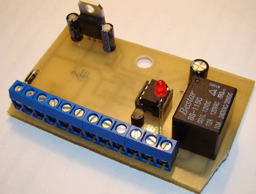
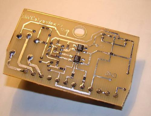
8. What, in the end, happened.
And to make things easier for you, I made a video lesson on the production of printed circuit boards using the Laser Iron method aka LUT.
A complete cycle, from the preparation of a board from a piece of textolite, to drilling and tinning.
What is needed:
0) Picture of the printed circuit board in electronic form.
1) Laser printer, to print the print of the future board. It is desirable that the printer could have a direct path - printing with minimal bending of the paper. I have the Samsung ML1520. Print to maximum, without any toner savings!
2) Foiled textolite.
3) Inkjet Photo Paper Lomond 120g / m glossy, one-sided with an improved coating. Also good results on paper Lomond 230g / m glossy.
4) Brush for suede with metal + plastic pile (optional)
5) Acetone
6) Skin of nulling
The entire process was cut into operations for easy viewing, processing and downloading to the Internet. When making a board, between operations, the time period was a few minutes. Basically, it was spent looking for some cotton, acetone or tweezers to grab a hot board. So you can assume that they go without interruption in time to assess the speed of making boards.
1. Preparation of the fee.
2. Roll the drawing.
Our goal is to make a protective drawing on the printed circuit board, which will protect the tracks from etching in an aggressive metal solution of ferric chloride.
3. Remove the paper:
Soaking and disruption of paper, cleaning the glossy layer.
4. Pickling.
As a pickling solution, chlorine iron is used - an infernal thing that consumes almost all metals. The solution is made from a ratio of 250 g of ferric chloride per liter of water. Accuracy is not important here.
5. Removing the toner
Maurus did the work, the Moor must go.
6. Drilling holes.
7. Board tinning.
8. What, in the end, happened.

Comments
When commenting on, remember that the content and tone of your message can hurt the feelings of real people, show respect and tolerance to your interlocutors even if you do not share their opinion, your behavior in the conditions of freedom of expression and anonymity provided by the Internet, changes Not only virtual, but also the real world. All comments are hidden from the index, spam is controlled.