
Modern power lockable thyristors
Introduction
The creation of semiconductor devices for power electronics began in 1953 when it became possible to obtain silicon of high purity and the formation of silicon disks of large sizes. In 1955, a semiconductor controlled device was first created, which had a four-layer structure and was called the "thyristor".
It was switched on by applying a pulse to the control electrode at a positive voltage between the anode and the cathode. The switching off of the thyristor is provided by the reduction of the direct current flowing through it to zero, for which a number of circuits of inductive capacitive switching circuits have been developed. They not only increase the cost of the transformer, but also worsen its mass-dimensional indicators, reduce reliability.
Therefore, simultaneously with the creation of the thyristor, research has begun to ensure its shutdown by the control electrode. The main problem was to ensure a rapid resolution of the charge carriers in the base regions.
The first such thyristors appeared in 1960 in the USA. They are called Gate Turn Off (GTO). In our country they are better known as lockable or switched off thyristors.
In the mid-90's a lockable thyristor with a ring lead of the control electrode was developed. It was named Gate Commutated Thyristor (GCT) and became the further development of GTO-technology.
Thyristors GTO
Device
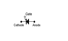
The lockable thyristor is a fully controllable semiconductor device, based on a classical four-layer structure. Turn it on and off by supplying positive and negative current pulses to the control electrode. In Fig. 1 shows the symbol (a) and the block diagram (b) of the switched-off thyristor. Like a conventional thyristor, it has a cathode K, an anode A, a control electrode G. Differences in instrument structures consist in a different arrangement of horizontal and vertical layers with n and p conductivities.
 |
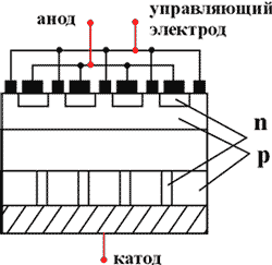 |
Fig. 1. Locked thyristor:
| |
The greatest change was in the arrangement of the cathode layer n. It is divided into several hundred elementary cells, evenly distributed over the area and connected in parallel. This performance is caused by the desire to ensure a uniform current reduction throughout the entire area of the semiconductor structure when the device is turned off.
The base layer p, despite being made as a whole, has a large number of contacts of the control electrode (approximately equal to the number of cathode cells) also uniformly distributed over the area and connected in parallel. The base layer n is made similar to the corresponding layer of a conventional thyristor.
The anode layer p has shunts (zones n) connecting the n-base to the anodic contact through small distributed resistances. Anode shunts are used in thyristors that do not have an inverse blocking ability. They are designed to reduce the turn-off time of the device by improving the conditions for the extraction of charges from the base region n.
The main version of the GTO thyristor is a tablet with a four-layer silicon wafer clamped through heat-compensating molybdenum disks between two copper bases with increased thermal and electrical conductivity. With a silicon plate, a control electrode is contacted, having a terminal in the ceramic body. The device is clamped by contact surfaces between two halves of coolers, isolated from each other and having a design determined by the type of cooling system.
Operating principle
In the cycle of operation of the thyristor GTO, four phases are distinguished: inclusion, conductive state, shutdown and blocking state.
At the schematic section of the thyristor structure (Fig. 1, b), the lower terminal of the structure is anodic. The anode contacts the layer p. Subsequently, the bottom layer is followed by: a base layer n, a base layer p (having a control electrode terminal), a layer n directly in contact with the cathode terminal. Four layers form three pn junctions: j1 between the layers p and n; J2 between the layers n and p; j3 between the layers p and n.
Phase 1 - inclusion. The transition of the thyristor structure from the blocking state to the conducting state (inclusion) is possible only when a forward voltage is applied between the anode and the cathode. Transitions j1 and j3 shift in the forward direction and do not interfere with the passage of charge carriers. All voltage is applied to the middle j2 junction, which is shifted in the opposite direction. Near the j2 junction, a zone depleted by the charge carriers is formed, which has been called the region of the bulk charge. To turn on the thyristor GTO, a voltage of positive polarity U G (pin "+" to layer p) is applied to the control electrode and cathode along the control circuit. As a result, the on-current I G flows through the circuit.
Lockable thyristors impose strict requirements on the steepness of the front dIG / dt and the amplitude of the IGM control current. Through the j3 junction, in addition to the leakage current, the switching current I G begins to flow. The electrons creating this current will be injected from layer n to layer p. Next, some of them will be transferred by the electric field of the base j2 transition to the layer n.
At the same time, counter injection of holes from the layer p into the layer n and further into the layer p, will increase simultaneously. There will be an increase in the current created by the minority charge carriers.
The total current passing through the base j2 transition exceeds the on-current, the thyristor is opened, after which the charge carriers freely pass through all four of its regions.
Phase 2 is a conducting state. In the direct current flow mode, there is no need for a control current I G , if the current in the anode circuit is higher than the holding current. However, in practice, in order to ensure that all structures of the switched-off thyristor are constantly in a conducting state, it is still necessary to maintain the current provided for the given temperature regime. Thus, the control system generates a current pulse of positive polarity all the time of switching on and conducting state.
In the conducting state, all regions of the semiconductor structure ensure a uniform motion of charge carriers (electrons from the cathode to the anode, holes in the opposite direction). Through the j1, j2 junctions, the anode current flows, and j3 is the total current of the anode and the control electrode.
Phase 3 - shutdown. To turn off the thyristor GTO with the voltage U T is unchanged (see Fig. 3), a voltage of negative polarity UGR is applied to the control electrode and cathode along the control circuit. It causes an off-current, the flow of which leads to the resorption of the main charge carriers (holes) in the base layer p. In other words, there is a recombination of holes entering the layer p from the base layer n, and electrons entering the same layer along the control electrode.
As the basic transition j2 is released from them, the thyristor begins to be locked. This process is characterized by a sharp decrease in the forward current I th of the thyristor in a short time interval to a small value I TQT (see Fig. 2). Immediately after locking the base j2 j3, the j3 transition begins to close, but for some time due to the energy stored in the inductance of the control circuits it is in a slightly open state.
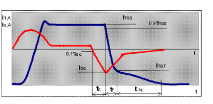
Fig. 2. Graphs of the current change of the anode (iT) and the control electrode (iG)
After all the energy stored in the inductance of the control circuit is consumed, the j3 transition from the side of the cathode is completely locked. From now on, the current through the thyristor is equal to the leakage current that flows from the anode to the cathode through the control electrode circuit.
The process of recombination and, consequently, shutdown of the lockable thyristor largely depends on the steepness of the front dIGQ / dt and the amplitude I GQ of the reverse control current. To ensure the necessary steepness and amplitude of this current, a voltage UG must be applied to the control electrode, which should not exceed the value permissible for j3.
Phase 4 - the blocking state. In the blocking state, the voltage of the negative polarity U GR from the control unit remains attached to the control electrode and cathode. The control current flows the total current I GR , consisting of the leakage current of the thyristor and the reverse control current passing through j3. The j3 transition shifts in the opposite direction. Thus, in a GTO thyristor in a forward blocking state, two junctions (j2 and j3) are biased in the opposite direction and two space charge regions are formed.
All the time of shutdown and blocking state control system generates a pulse of negative polarity.
Protective chains
The use of thyristors GTO, requires the use of special protective circuits. They increase the mass-dimensions, the cost of the converter, sometimes require additional cooling devices, but are necessary for the normal functioning of the devices.
The purpose of any protective circuit is to limit the rate of increase of one of the two parameters of electrical energy when switching a semiconductor device. In this case, the capacitors of the protective circuit CB (Figure 3) are connected in parallel to the protected device T. They limit the rate of rise of the direct voltage dUT / dt when the thyristor is turned off.
LE chokes are installed in series with the device T. They limit the rate of rise of the direct current dIT / dt when the thyristor is switched on. The values of dUT / dt and dIТ / dt for each device are normalized, they are indicated in the manuals and the passport data for the instruments.
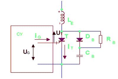
Fig. 3. Scheme of the protective circuit
In addition to capacitors and chokes, additional circuits are used in protective circuits to ensure the discharge and charge of reactive elements. These include: the diode DB, which shunts the resistor RB when the thyristor T is switched off and the capacitor CB is charged, the resistor RB, which limits the discharge current of the capacitor CB when the thyristor T is turned on.
Control system
The control system (CU) comprises the following functional blocks: a contour consisting of a circuit for generating a gate pulse and a signal source for maintaining the thyristor in an open state; Blocking circuit; Circuit maintaining the thyristor in a closed state.
Not all types of CS need all of the listed blocks, but the contours of the formation of the unlocking and locking pulses must contain each SS. In this case, it is necessary to ensure galvanic isolation of the control circuit and the power circuit of the switched-off thyristor.
To control the operation of a switched-off thyristor, two main SSs are used, differing in the ways of signal feeding to the control electrode. In the case shown in Fig. 4, the signals generated by the logic unit St are galvanically isolated (separation of potentials), and then they are fed through the switches SE and SA to the control electrode of the switched-off thyristor T. In the second case, the signals first act on the switches SE (on) and SA (off ), Which are at the same potential as the SS, then are fed to the control electrode through the galvanic isolation devices UE and UA.
Depending on the location of the keys SE and SA distinguish low-potential (NPSU) and high-potential (SSP, Figure 4) control schemes.
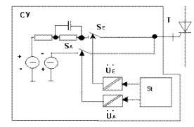
Fig. 4. Control circuit variant
The control system of the NPSU is structurally simpler than the VSPU, but its capabilities are limited in the formation of control signals of long duration, operating in the regime in the flow through the thyristor of the forward current, and also in ensuring the steepness of the control pulses. To generate long-duration signals, we have to use more expensive two-stroke circuits.
In the VPSU, the high steepness and the increased duration of the control signal are achieved more simply. In addition, here the control signal is used in full, while in the NPSU its value is limited by the potential separation device (for example, by a pulse transformer).
Information signal - a command to switch on or off - is usually fed to the circuit via an optoelectronic converter.
GCT thyristors
In the mid-1990s, ABB and Mitsubishi developed a new type of Gate Commutated Thyristor (GCT). Actually, GCT is a further improvement of the GTO, or its modernization. However, a fundamentally new design of the control electrode, as well as noticeably different processes that occur when the device is switched off, make it expedient to consider it.
GCT was designed as a device without the drawbacks typical of the GTO, so first you need to stop on the problems that arise when working GTO.
The main disadvantage of GTO is the large energy losses in the protective circuits of the device when it is switched. Increasing the frequency increases the losses, so in practice the thyristors GTO are switched at a frequency of no more than 250-300 Hz. The main losses occur in the resistor RB (see Figure 3) when the thyristor T is turned off and, consequently, the discharge of the capacitor CB.
The capacitor CB is designed to limit the rate of rise of the direct voltage du / dt when the device is turned off. By making the thyristor not sensitive to the du / dt effect, it was possible to abandon the snubber circuit (the switching path forming circuit), which was implemented in the GCT design.
Feature of control and design
The main feature of GCT thyristors, in comparison with GTO devices, is a rapid shutdown, which is achieved both by changing the control principle and by improving the design of the device. Fast turn-off is realized by turning the thyristor structure into a transistor structure when the device is locked, which makes the device not sensitive to the du / dt effect.
GCT in the phases of switching on, conducting and blocking states is controlled as well as GTO. When you turn off the control GCT has two features:
- The control current Ig is equal to or exceeds the anode current Ia (for thyristors GTO Ig less than 3 to 5 times);
- The control electrode has a low inductance, which makes it possible to achieve a dig / dt control current increase rate of 3000 A / μs and more (for digitizers GTO, the dig / dt value is 30-40 A / μs).
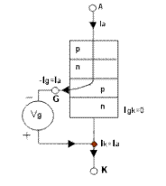
Fig. 5. Distribution of currents in the structure of the thyristor GCT at shutdown
In Fig. 5 shows the current distribution in the GCT thyristor structure when the device is turned off. As indicated, the actuation process is similar to the inclusion of thyristors GTO. The shutdown process is different. After a negative control pulse (-Ig) of an equal magnitude of the anode current (Ia) is applied, all the forward current passing through the device is diverted into the control system and reaches the cathode, bypassing the j3 transition (between the regions p and n). The j3 transition is shifted in the opposite direction, and the cathode transistor npn is closed. Further switching off the GCT is analogous to turning off any bipolar transistor, which does not require external limitation of the rate of rise of the forward voltage du / dt and, therefore, allows the absence of a snubber chain.
The change in the design of GCT is due to the fact that the dynamic processes occurring in the device during shutdown proceed one to two orders faster than in the GTO. So, if the minimum turn-off time and the blocking state for the GTO is 100 μs, for GCT this value does not exceed 10 μs. The rate of increase of the control current when switching off the GCT is 3000 A / μs, GTO - does not exceed 40 A / μs.
To ensure high dynamics of switching processes, the design of the output of the control electrode and the connection of the device with the pulse driver of the control system were changed. The output is made circular, circling the device around the circumference. The ring passes through the ceramic body of the thyristor and contacts: inside with the cells of the control electrode; Outside - with a plate connecting the control electrode with the pulse former.
Now the GTO thyristors are produced by several large companies of Japan and Europe: "Toshiba", "Hitachi", "Mitsubishi", "ABB", "Eupec". Parameters of devices for voltage UDRM: 2500 V, 4500 V, 6000 V; Current ITGQM (maximum repeating lockable current): 1000 A, 2000 A, 2500 A, 3000 A, 4000 A, 6000 A.
GCT thyristors are manufactured by Mitsubishi and ABB. The devices are designed for voltage UDRM up to 4500 V and current ITGQM up to 4000 A.
Currently, thyristors GCT and GTO are mastered at the Russian enterprise JSC "Electrovypryamitel" (Saransk). Thyristors of the series TZ-243, TZ-253, TZ-273, ZTA-173, ZTA-193, ZTF-193 (similar to GCT ) And others with a silicon wafer diameter of up to 125 mm and a voltage range of UDRM 1200 - 6000 V and currents ITGQM 630 - 4000 A.
In parallel with the lockable thyristors and for use in conjunction with them, JSC "Electrovypryamitel" developed and mastered in series production fast-setting diodes for damping (snubber) circuits and reverse current diodes, as well as a powerful pulse transistor for output stages of the driver of control (control system).
Thyristors IGCT
Thanks to the concept of rigid control (thin regulation of alloying profiles, meza- technology, proton and electron irradiation for the creation of a special distribution of controlled recombination centers, the technology of so-called transparent or thin emitters, the use of a buffer layer in the n-base region, etc.) When turning off. The next major achievement in the technology of rigidly controlled GTO (HD GTO) in terms of instrumentation, control and application was the idea of controlled devices based on a new "locked thyristor with an integrated control unit (driver)" (English Integrated Gate-Commuted Thyristor (IGCT)) . Thanks to the hard control technology, uniform switching increases the safe working area of the IGCT to the limits limited by avalanche breakdown, i. E. To the physical capabilities of silicon. No protective circuits are required from exceeding du / dt. The combination with improved power losses allowed us to find new applications in the kHz range. The power required for control is reduced by a factor of 5 compared to the standard GTO, mainly due to the transparent design of the anode. The new IGCT family of monolithic integrated high-power diodes has been developed for use in the range 0.5 - 6 MVA. With the existing technical capability of serial and parallel connection, IGCT devices allow to increase the power level up to several hundred megavolts - amperes.
With the integrated control unit, the cathode current is reduced before the anode voltage begins to increase. This is achieved due to the very low inductance of the control electrode circuit, realized due to the coaxial connection of the control electrode in combination with the multilayer board of the control unit. As a result, it became possible to achieve the value of the switched-off current rate of 4 kA / μs. With a control voltage UGK = 20 V. When the cathode current becomes zero, the remaining anode current goes to the control unit, which at this time has a low resistance. Due to this, the energy consumption of the control unit is minimized.
Working with "hard" control, the thyristor switches when locked from pnpn state to pnp mode for 1 us. The shutdown occurs completely in the transistor mode, eliminating any possibility of triggering the trigger effect.
Reducing the thickness of the device is achieved by using a buffer layer on the anode side. The buffer layer of power semiconductors improves the characteristics of traditional elements by reducing their thickness by 30% with the same direct breakdown voltage. The main advantage of thin elements is the improvement of technological characteristics at low static and dynamic losses. Such a buffer layer in a four-layer instrument requires the elimination of anode short circuits, but at the same time the effective release of electrons during the shutdown is preserved. In the new IGCT device, the buffer layer is combined with a transparent anode emitter. A transparent anode is a pn junction with a current-controlled emitter efficiency.
For maximum noise immunity and compactness, the control unit surrounds the IGCT, forming a single structure with a cooler, and contains only that part of the circuit that is needed to control the IGCT directly. As a consequence, the number of elements of the control unit is reduced, the parameters of heat dissipation, electrical and thermal overloads are reduced. Therefore, the cost of the control unit and the failure rate are also significantly reduced. The IGCT, with its integrated control unit, is easily fixed in the module and precisely connected to the power source and control signal source via the fiber. By simply opening the spring, thanks to the elaborate clamping contact system, a correctly designed clamping force is applied to the IGCT, creating electrical and thermal contact. Thus, the maximum ease of assembly and the greatest reliability are achieved. When IGCT operates without a snubber, the reverse diode must also work without a snubber. These requirements are fulfilled by a high-power diode in a clamping casing with improved characteristics, manufactured using the irradiation process in combination with classical processes. The di / dt capabilities are determined by the operation of the diode (see Figure 6).
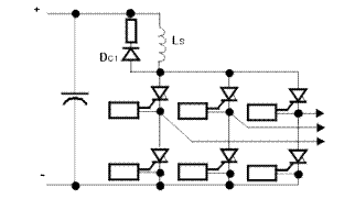
Fig. 6. Simplified three-phase inverter circuit for IGCT
The main manufacturer of IGCT firm "ABB". Parameters of thyristors for voltage U DRM : 4500 V, 6000 V; The current ITGQM: 3000 A, 4000 A.
Conclusion
The rapid development of power transistor technology in the early 1990s led to the emergence of a new class of devices - IGBTs - Insulated Gate Bipolar Transistors. The main advantages of IGBT are high operating frequency, efficiency, simplicity and compactness of control circuits (due to small control current).
The appearance in recent years of the IGBT with an operating voltage of up to 4500 V and the ability to commute currents to 1800 A has led to the displacement of locked-in thyristors (GTO) in devices up to 1 MW and a voltage of up to 3.5 kV.
However, the new IGCTs, capable of operating at switching frequencies from 500 Hz to 2 kHz and having higher parameters than IGBT transistors, combine an optimal combination of proven thyristor technologies with their inherent low losses, and a powerless, high-efficiency shutdown technology by affecting Control electrode. The IGCT device today is the ideal solution for applications in the field of power electronics of medium and high voltage.
Characteristics of modern powerful power switches with two-sided heat dissipation are given in Table. 1.
Table 1. Characteristics of modern powerful power switches with two-sided heat sink
| Device type | Benefits | disadvantages | Areas of use |
| Traditional thyristor (SCR) | Lowest losses in the on state. The highest overload capacity. High reliability. Easily connect in parallel and in series. | Not capable of forced locking on the control electrode. Low operating frequency. | DC drive; Powerful power supplies; welding; Melting and heating; Static compensators; Alternating current switches |
| GTO | Ability to controllable locking. Relatively high overload capacity. Possibility of serial connection. Operating frequencies up to 250 Hz at a voltage of up to 4 kV. | High loss in the on state. Very large losses in the control system. Complex control systems and power supply for the potential. Great loss on switching. | The electric drive; Static compensators; reactive power; Uninterruptible power systems, induction heating |
| IGCT | Ability to controllable locking. The overload capacity is the same as that of the GTO. Low losses in the on state for switching. The operating frequency is up to units, kHz. Built-in control unit (driver). Possibility of serial connection. | Not identified due to lack of operational experience | Powerful power supplies (inverter and rectifier substations of DC transmission lines); Electric drive (voltage inverters for frequency converters and electric drives for various purposes) |
| IGBT | Ability to controllable locking. The highest operating frequency (up to 10 kHz). Simple non-energy management system. Built-in driver. | Very high losses in the on state. | Electric drive (choppers); Uninterruptible power supply systems; Static compensators and active filters; Key power supplies |

Comments
Commenting on, remember that the content and tone of your message can hurt the feelings of real people, show respect and tolerance to your interlocutors even if you do not share their opinion, your behavior in the conditions of freedom of expression and anonymity provided by the Internet, changes Not only virtual, but also the real world. All comments are hidden from the index, spam is controlled.