| Start of section
Production, amateur Radio amateurs Aircraft model, rocket-model Useful, entertaining |
Stealth Master
Electronics Physics Technologies Inventions |
Secrets of the cosmos
Secrets of the Earth Secrets of the Ocean Tricks Map of section |
  |
| Use of the site materials is allowed subject to the link (for websites - hyperlinks) | |||
Navigation: => |
Home / Table of Contents / Table of Contents / |
|
NEW METHOD OF MANAGING TRANSISTOR
Valery Rudenko
The invention relates to electronics. The technical result is the creation of short-term high-amplitude pulses. The method for controlling the transistor cascade, in which the inductance is included in the controlled collector-emitter circuit, consists in creating a mode in which the bias voltage in the transistor base constantly keeps the transistor in the cut-off mode, while the collector-emitter voltage becomes smaller than the base-emitter voltage, the base The collector transition remains backward biased and a potential barrier arises for carrier transitions from the base to the collector, which creates conditions for the gradual accumulation of a space charge in the base region, which becomes a conducting channel for the short-circuit current between the poles of the power supply source of the transistor cascade through the inductance And transitions of the transistor.

DESCRIPTION OF THE INVENTION
The invention relates to the field of electronics. The disadvantage of the known method of controlling the transistor is the inability to create short-term high-amplitude pulses, because the generation and resolution of carriers formed in the base require a certain time interval commensurate with the duration of the short pulse. Another disadvantage is the inability to transmit information from one stage of the transistor to the other without galvanic coupling between the cascades.
The prototype of the present invention can be adopted by a blocking generator (LM Gol'dberg, Pulsed and Digital Devices, Communication, 1973, Chapter 6). It is a generator with inductances in the collector and in the base, covered by positive feedback, in which the process of changing the current in the base stops when saturation is reached in the ferromagnetic core. Such a method does not allow receiving pulses in the absence of a ferromagnetic core in the transformer, and although it provides a transformer coupling, but only through the core, in addition, pulses of the nanosecond range of duration from the blocking generator can not be obtained. Resonance amplifiers on air transformers provide a transformer coupling, but only at a resonant frequency. Therefore, in the prior art, the above disadvantages are not overcome.
The proposed control method allows to overcome these drawbacks with the help of inductance and a number of techniques that are the subject of the present invention.
According to Lenz, Faraday, EMF self-inductance in the inductance is directed towards the current, its causing (referring to the base and collector currents arising in the locked transistor), and its amplitude can be commensurable with the voltage of the power source. If the inductance is included in the controllable (collector-emitter) circuit of the transistor cascade, then a regime is created at which the voltage Uke becomes smaller than Ube, and the base-collector transition is reversed, and a potential barrier arises for carriers to migrate from the base to the collector. Numerically, it looks like Uke = 0.1 V, Ube = 0.6 V for a silicon transistor npn. This creates the conditions for a gradual, during a considerable period of time, accumulation in the region of the base of the space charge of the carriers. And this happens in a locked transistor.
When the base is overfilled with carriers, it becomes a conducting channel for the short-circuit current between the poles of the power source through the inductance and the collector-emitter of the transistor.
The source of the displacement of the base causes injection of carriers from the emitter, and with the appearance of carriers in the volume of the base adjacent to the emitter, the potential having the sign of injected carriers opposite in sign to the source of displacement increases, and therefore the current of the base will decrease, with the base current passing through 0, potentials Internal and external from the source of displacement will be equalized (see Fig. 1). With the increase of the internal potential, the potential barrier created at the base-collector transition will be overcome, and at that moment conditions for a short circuit from the power source through the collector-emitter and inductance are created.
The current through the inductance and the collector-emitter, the amplitude of which is determined by the resistance of the circuit, and its duration - the number of carriers stored in the base and dragged from the base volume by the electric field of the power source, is a short-circuit current because the inductance and transistor resistance is close to zero Ohm . This allows the output of short-term high-amplitude current pulses.
After the removal from the base of the mobile carriers by the collector current generated from the previously accumulated space charge, its resistance sharply increases (the bias voltage in the base can be constant and keeps the transistor in cut-off mode) and this is accompanied by the response of the self-inductance EMF of the controllable (collector) In the opposite direction.
The backward reaction pulse of the inductance current neutralizes the sources of carrier generation in the emitter, and the larger the EMF pulse amplitude, the more sources of carrier generation are covered by neutralization, the resistance of the transitions increases and is close to infinity. From this, the pause between the short-circuit pulses consisting of the inductor power supply and the transistor transitions becomes longer. The event occurs periodically: first the accumulation of the charge (the number of carriers of FIG. 1b, the 1st interval), then the current pulse through the inductance (FIG. 1b 2nd interval), then the reverse reaction with suppression of the generation sources (FIG. 1d, 3rd interval) And repetition of the process.
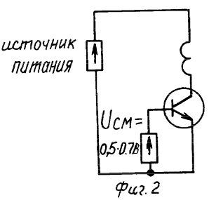
In one of the variants (FIG. 2) of the execution of the driver (the author gave such a name to devices operating on the claimed control method), the cascade can consist of one collector inductor, and at the base-emitter junction of the silicon transistor, a direct bias is established using an external source with a voltage of 0.5- 0.7 volts, while the transistor is held in the cutoff mode.
In a similar case, if another inductance is set on the base contact (Fig. 2), the amplitude of the reverse reaction will become different due to mutual induction. The duration of the accumulation period of the space charge in the base will increase if the coils of the base and collector coils are turned inverted, or decrease, if - according to.
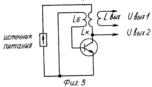
In the current understanding, the circuit (FIG. 3) can not operate as a generator, since the basic circuit is locked, because There is no positive offset in the database. And nevertheless, it works as a pulse generator, because the positive half-wave serves as a bias, and this circuit generates self-starting with germanium bipolar, field, transistors and a p / lamp. It also works with a silicon transistor, but only with an external trigger, through a transformer link, with the help of another driver.
On the diagrams of Fig. 1, in the second interval there is no trace of the short-circuit current, since the space charge is discharged due to the removal of only the carriers accumulated during the 1-st interval from the base region and the transfer of the energy of the accumulated carriers to the magnetic flux of inductance Lk.
Therefore, considering the oscilloscope of the emf of carrying carriers to Lk and Lb with respect to the current from the positive and negative poles of the power supply (Fig. 1c, d), we see in the 2nd and 3rd interval the invariant polarity of the pulses at Uke and Ube. For transistors npn, it is positive, pnp is negative in the collector Uout2. On the basis of the pulse sign, the reverse is Ube in the 3 rd interval, and its polarity is the same when considering the positive and negative poles of the power source.
The current of the base 1b is decreasing (Fig. 1a), since Ube is applied to the directly displaced pn junction. In the base with the accumulation of carriers, the intrinsic potential of the base region grows, and the potential created by the winding Lb with the potential growing in the base region due to the accumulation of carriers in it, and changing the sign due to overcoming the potential barrier in the collector-base transition, is compensated.
In the 3 rd interval, a reverse polarity pulse is observed in the base (Fig. 1d), caused by the reverse reaction of the discharge pulse. It neutralizes the sources of carrier generation in the emitter. The subsequent restoration of the generation of carriers causes a repetition of the process.
As established experimentally by the author, the mutual induction between the base and other (collector, output, emitter) inductances can be realized not only according to the laws of Ampere and Bio-Savar, i.e. Not only through the magnetic field of the main current flowing through the inductance, but also through the magnetic moments of the atoms surrounding the inductor. In other words, the distance between the inductances in the base and collector circuits can be arbitrarily large, much larger than the sizes of the coils of inductances. The number of turns can vary in large limits, starting with one. Inductances can be either chip or wicker of arbitrary sizes. The interaction energy between the output and the collector inductors decreases linearly, and not inversely, as should be the Ampere law.
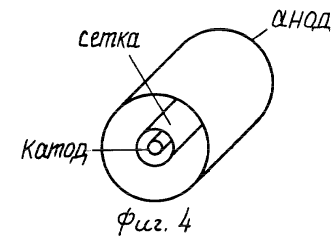
The method can be more clearly illustrated by the example of a radio-tube triode with an inductance in the anode.
If, due to the EMF self-induction in the anode circuit, the grid-cathode voltage is greater than the anode-cathode, then electrons will accumulate in the space between the cathode and the grid, which will fill the entire space between the grid and the cathode. Having escaped the limits of the cathode-grid volume, electrons will be carried away by the electric field of the anode. Through the inductance, the anode, the grid and the cathode, the circuit will close until the electrons from the cathode-grid space are removed and the inductance reacts with a jump in the EMF of the reverse polarity, which will lower the cathode output level, and the process of electron accumulation in the cathode-grid volume Will be repeated (FIG. 4).
The author has developed about 20 schemes of kachepers, some of them are given in the present application (FIGS. 2, 3, 5, a and see RF patent No. 2075726 and brochure Brovin VI "The phenomenon of transfer of energy inductivities through the magnetic moments of a substance In the surrounding space, and its application "M. Metasintez, 2003). They are all different, but they share one common principle of action.

CLAIM
A method for controlling a transistor cascade, in the controlled collector-emitter circuit of which the inductance is included, which consists in creating a mode in which the bias voltage in the transistor base keeps the transistor in the cut-off mode, while the collector-emitter voltage becomes less than the base-emitter voltage, the base The collector transition remains backward biased and a potential barrier arises for carrier transitions from the base to the collector, which creates conditions for the gradual accumulation of a space charge in the base region, which becomes a conducting channel for the short-circuit current between the poles of the power supply source of the transistor cascade through the inductance And transitions of the transistor.
print version
Author: Valery Rudenko
PS The material is protected.
Date of publication 09/21/2006
![]()

Comments
When commenting on, remember that the content and tone of your message can hurt the feelings of real people, show respect and tolerance to your interlocutors even if you do not share their opinion, your behavior in the conditions of freedom of expression and anonymity provided by the Internet, changes Not only virtual, but also the real world. All comments are hidden from the index, spam is controlled.